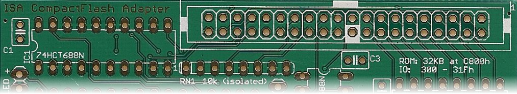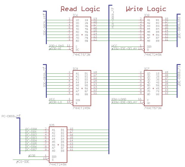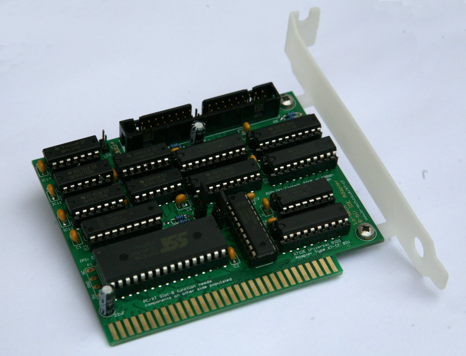

The Lo-tech 8-bit IDE Adapter is a bootable IDE controller for vintage PCs with only 8-bit ISA slots – basically PC/XT class hardware. The adapter is a development of the the Lo-tech ISA CompactFlash Adapter, adding an 8- to 16-bit MUX to make possible the use of normal hard drives, including current SATA drives (via an adapter like this). In this post, I’ll cover how to build the adapter and get it running.
Components
Here’s what’s in the kit bag:
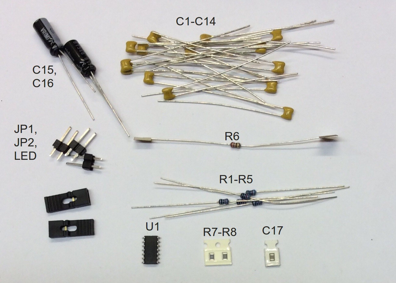
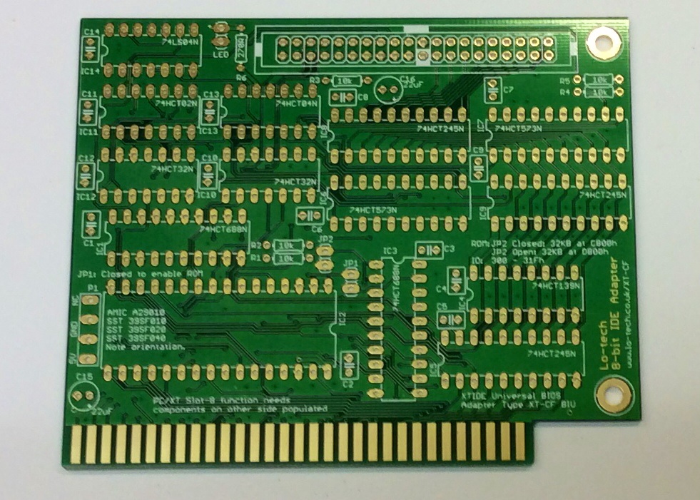
The only tricky parts are the SMT parts on the solder side of the board, basically a SOIC 74LS33D and a few resistors. These parts provide IBM PC/XT Slot-8 compatibility and enhanced read performance in PC/AT class systems, and can be simply left of if that functionality is not required.
The Build
Build order is basically determined by the height of the components, so that they’re held in place whilst soldering:
- SMT components first, if these are being used
- Resistors R1 to R6
- Capacitors C1 to C14
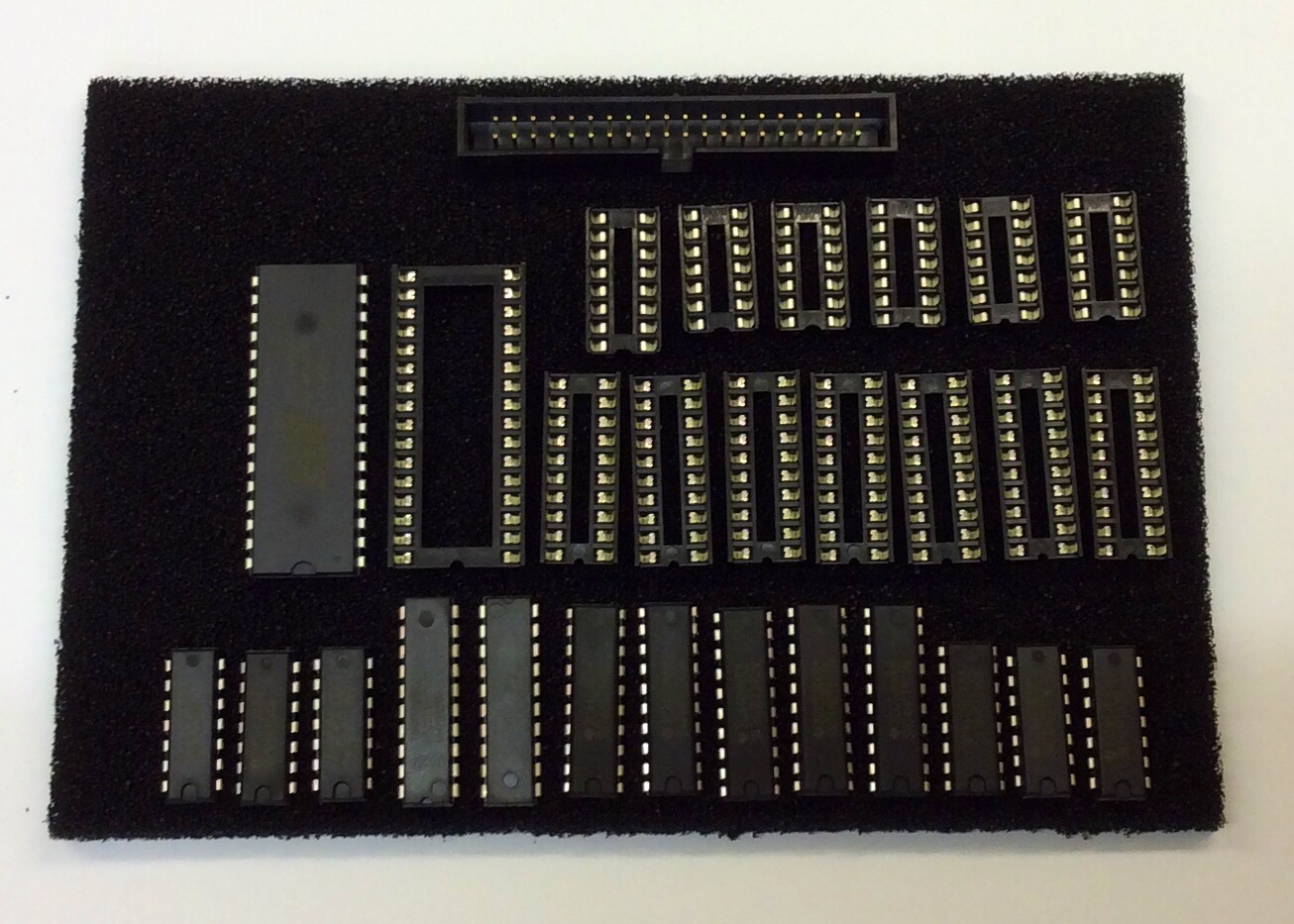
- IC sockets. Check correct orientation (the notch should line up with the notch shown on the board silkscreen). Solder one pin of each first, then check the sockets are properly against the board. Once two or more pins are soldered, they will be very difficult to remove.
- 2-pin headers JP1, JP2, LED. As with the sockets, solder one pin first and then check alignment.
- 40-pin header HD1. First remove the key pin from the header using some small pliers unless key-pin provided 5V power is required (for example, to power a directly connected SATA converter). Again, solder one pin and then check alignment. Work quickly on each pin to avoid overheating the header plastic, otherwise the pins can become misaligned.
At this point the board will have a lot of flux residue that needs to be thoroughly cleaned off:
The board can be cleaned by immersion in either warm de-ionised water, isopropynol, or a specific flux remover and gentle agitation with either a toothbrush or an ultrasonic cleaner. Once satisfactorily cleaned, the two electrolytic capacitors C15 and C16 should be added, and the respective soldering areas cleaned again.
Once cleaned, check the joints thoroughly for any dry-joints or bridges (shorts), particularly around the SMT components (if fitted).
Finishing the Board
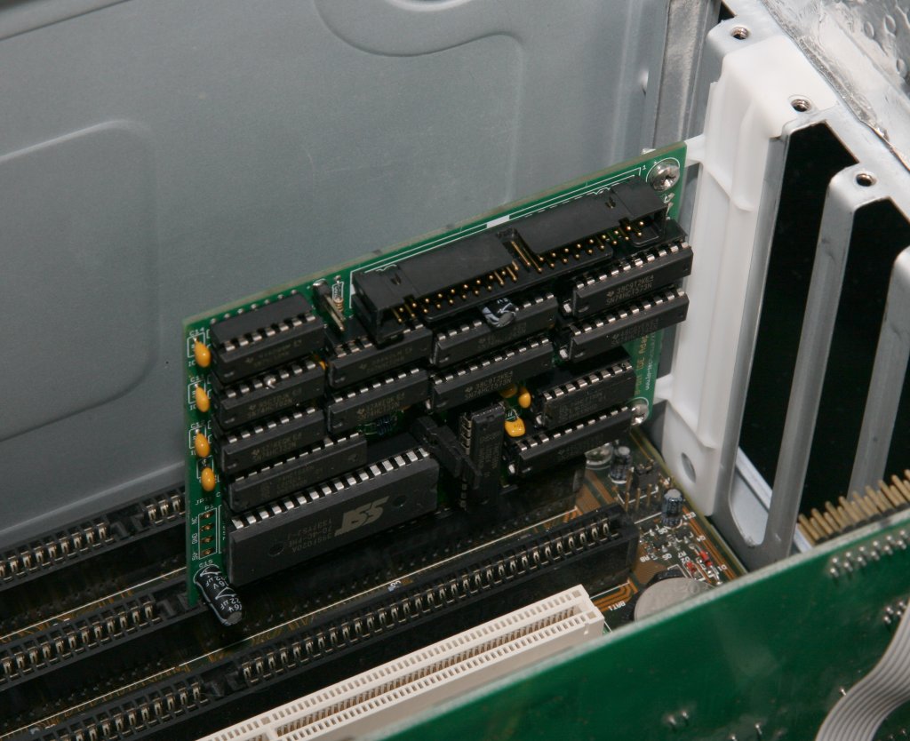
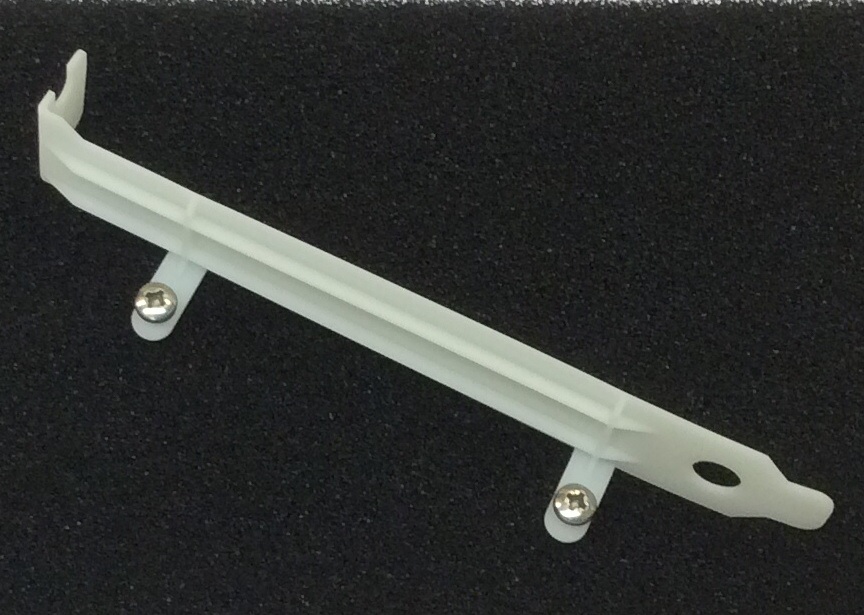
With the soldering done all that’s left to do is to dry thoroughly, for example with warm air (i.e. a hair dryer), add the ICs and slot bracket, then flash the BIOS.
Before the ICs can be fitted to the sockets, the pins need to be aligned using an alignment tool like this (ICs provided in Lo-tech kits are shipped ready aligned).
Errata
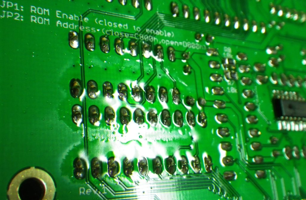
The first version of this board contains one error, which can be fixed by modifying the 74HCT02N that will be fitted as IC11 – pin 6 should be jumpered to pin 11, and pin 6 clipped or bent so it doesn’t make contact with the DIP socket. Here’s what the mod looks like (click on the images for a larger view) with the off-cut from a resistor used to make the connection:
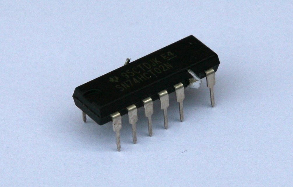
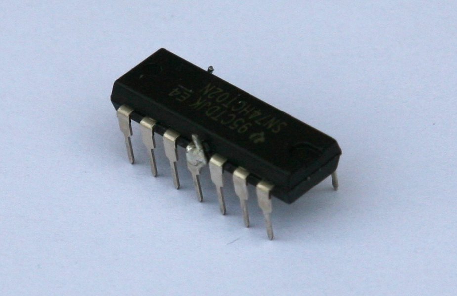
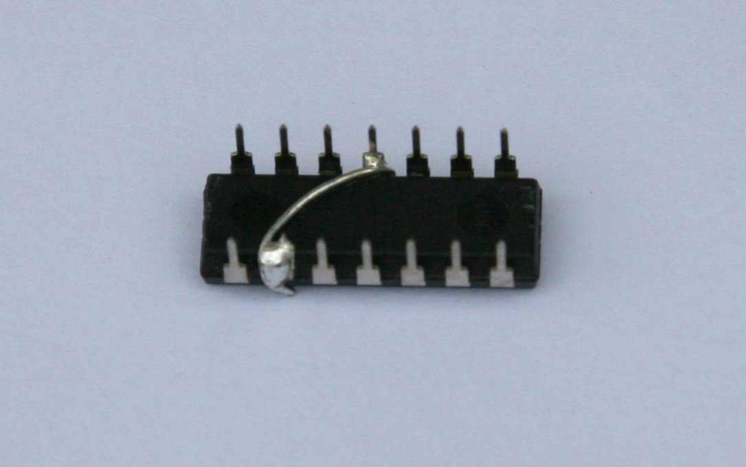
Without this modification, the write latch load signal is masked unless the request is port 0, which works for the data register but also means no commands can be issued to the drive! Instead, the signal should be masked only when the request is port 1, which as it happens is on pin 11 already. Note that this modification applies only to the first revision boards; no modifications are required for the Rev.2 board.
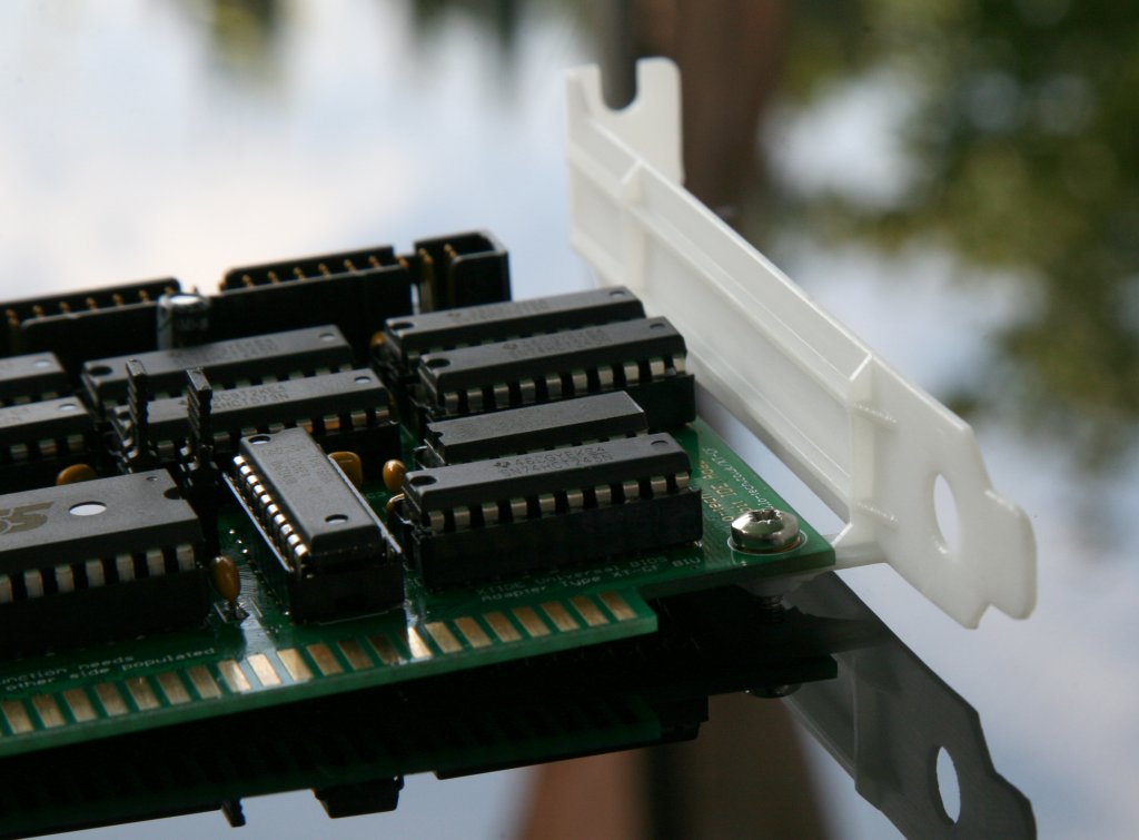
Mounting the Chips
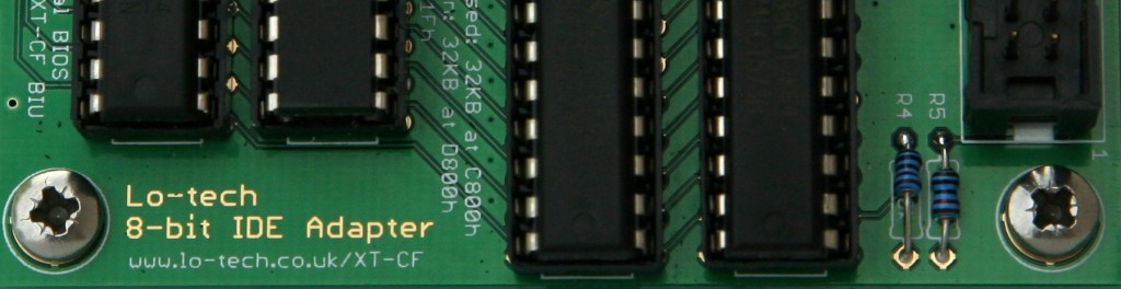
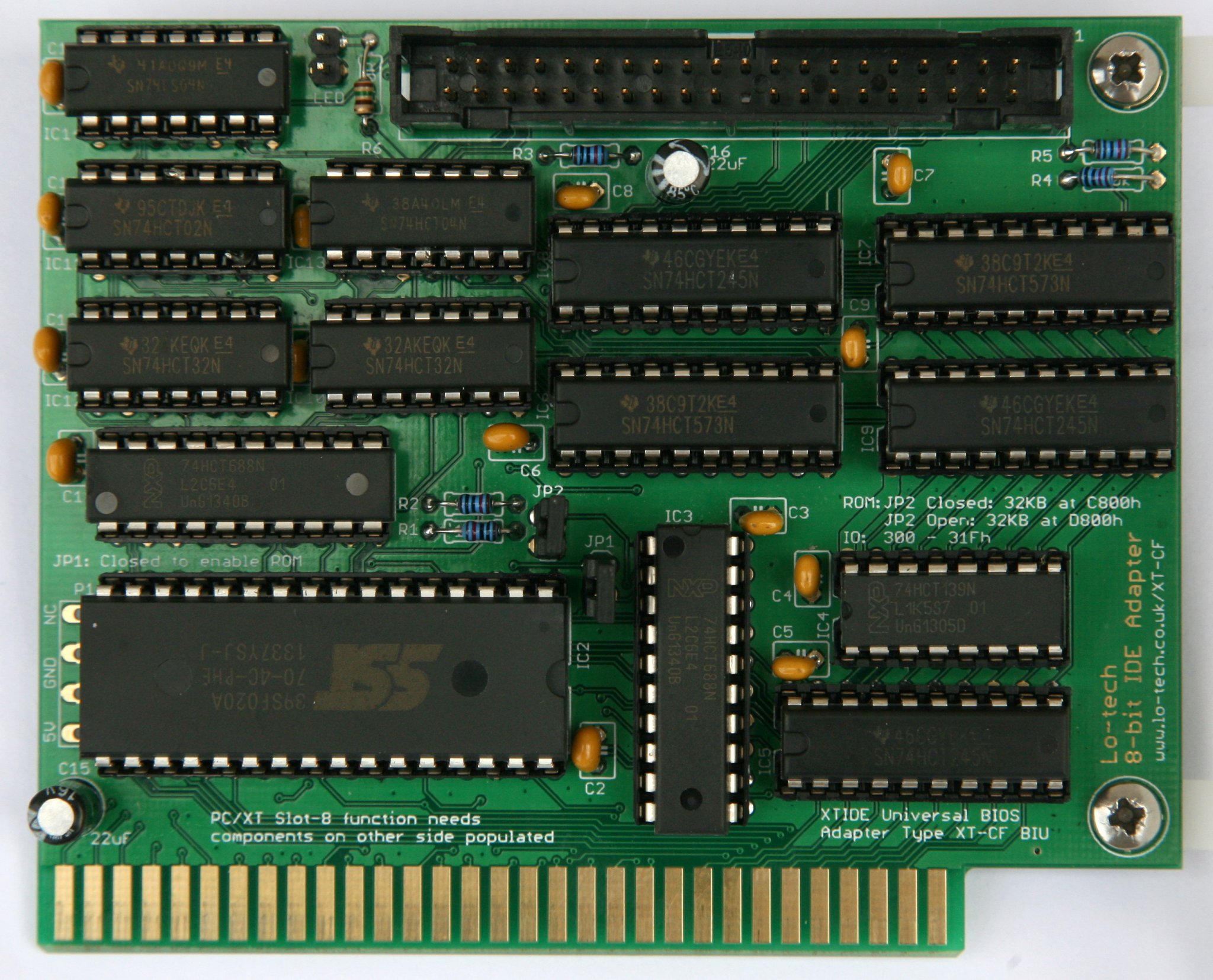
Once the pins are aligned, the chips can be mounted in the sockets, Ensure the chips are fitted in the correct orientation, shown by the notches. Here’s a finished board, for reference:
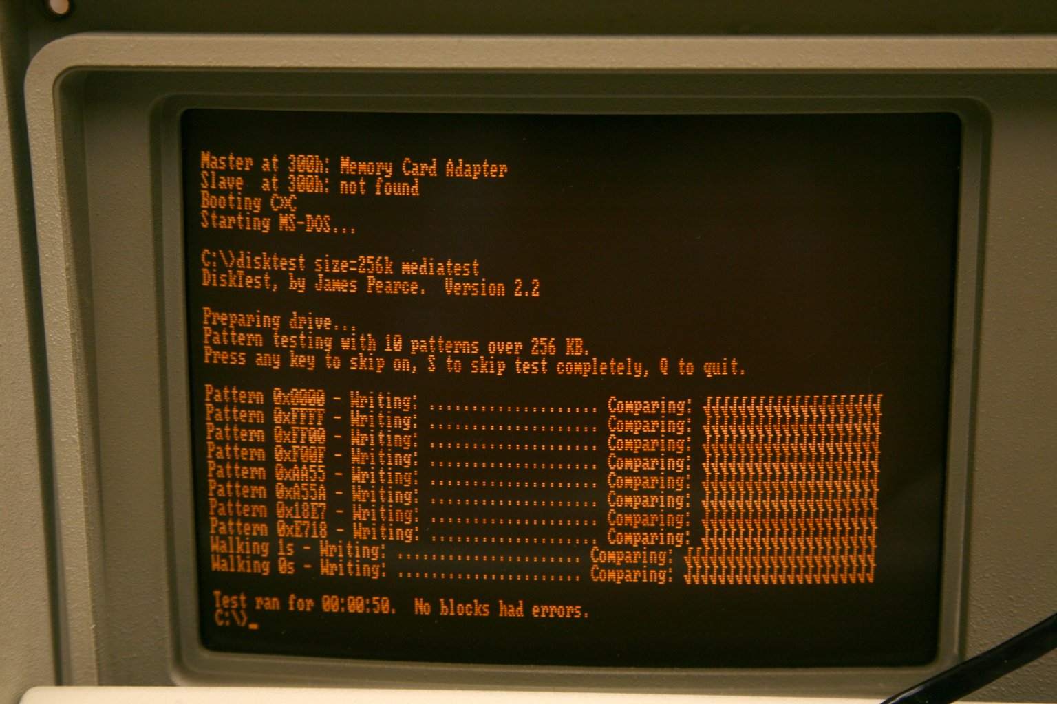
Flashing the BIOS and Testing
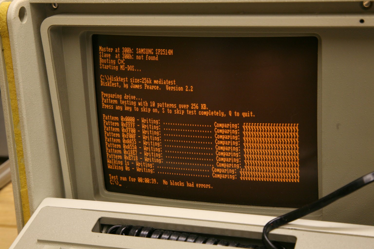
Once assembled and fitted in a PC, the BIOS needs to be stored in the flash chip on the card. There’s no external EPROM programmer needed – the chip can be flashed directly from DOS in the machine, using the Lo-tech FLASH utility.
Depending on how JP2 is set, the command needed is either (assuming the ROM image from the wiki is being used):
A:\>flash 8bit-ide.bin c800
or
A:\>flash 8bit-ide.bin d800
Once this has been done, reboot the PC and the XTIDE Universal BIOS should be displayed after the system POST, and any connected hard disks detected.
To get the machine to boot from the adapter, the primary disk will need to be partitioned (a primary and active partition created, using DOS FDISK utility) and then formatted (FORMAT C: /S). If the disk has been used with a newer operating system (anything other than DOS), a new Master Boot Record is probably needed as well, which can be created using DOS 6.22 by running FDISK /MBR.
PCB and Kit Availability
Rev.1 PCBs and kits are available in the store now – note these need one of the 74HCT02 chips modified as detailed above as part of the assembly process.
Lo-tech is in no way associated with the sellers of products on other sites linked to on this page (which are provided to provide an example of the types of products available).