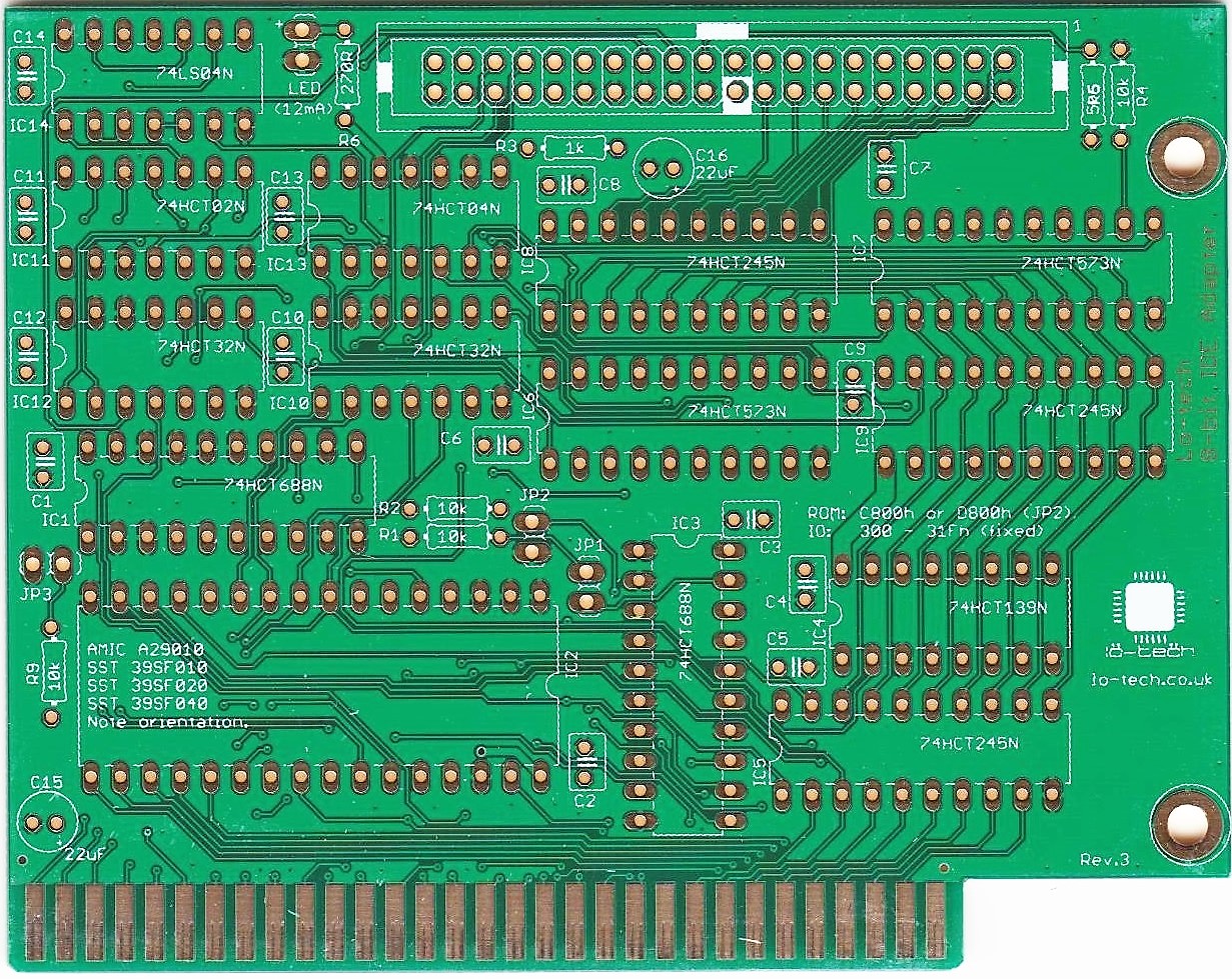
The Lo-tech 8-bit IDE adapter has been designed around a 3D-printed ISA slot bracket, the primary reason being to keep the card itself within a 100mm width, which helps keep the price down. Until now!
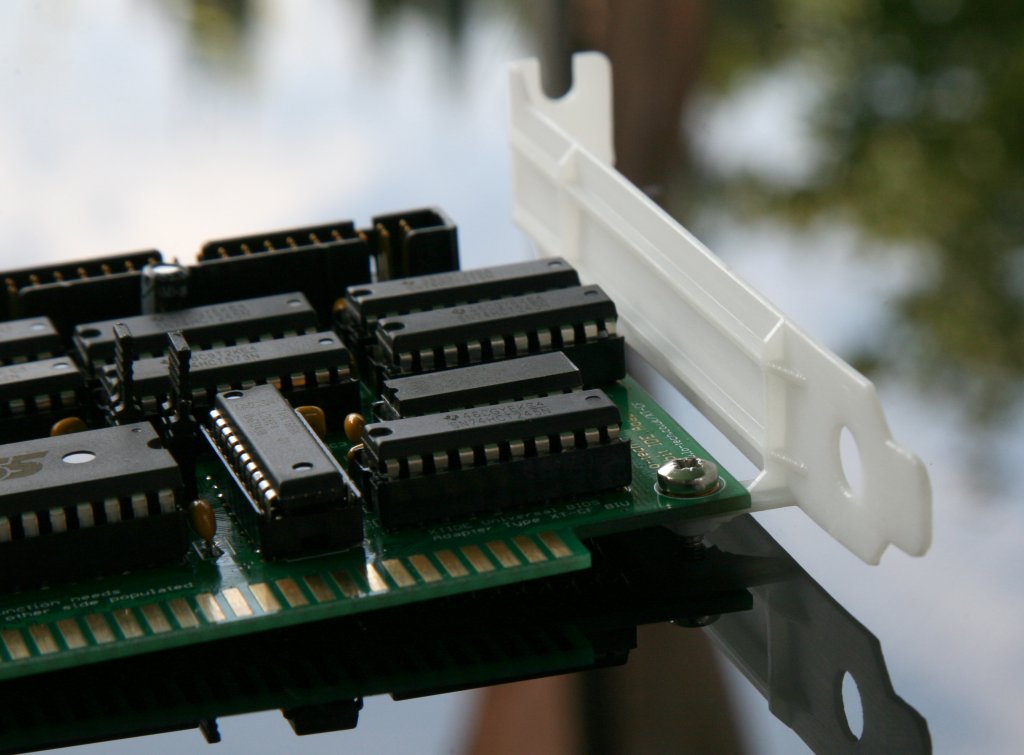
Announcing then the rev.3 board, which is now compatible with the Keystone 9202 ISA slot bracket, as available from the usual online electronics retailers such as Mouser.
As well as the slightly larger PCB form factor, this version also includes another jumper (JP3) providing a choice of IO ports, either the default 300h or 320h.
The board keeps everything else the same – XTIDE Universal BIOS powered, 32KB Flash ROM, excellent IDE and SATA device compatibility, high-speed read and write performance, key-pin power for Disk On Module devices, and PC/XT Slot-8 compatibility (with option SMT components fitted).
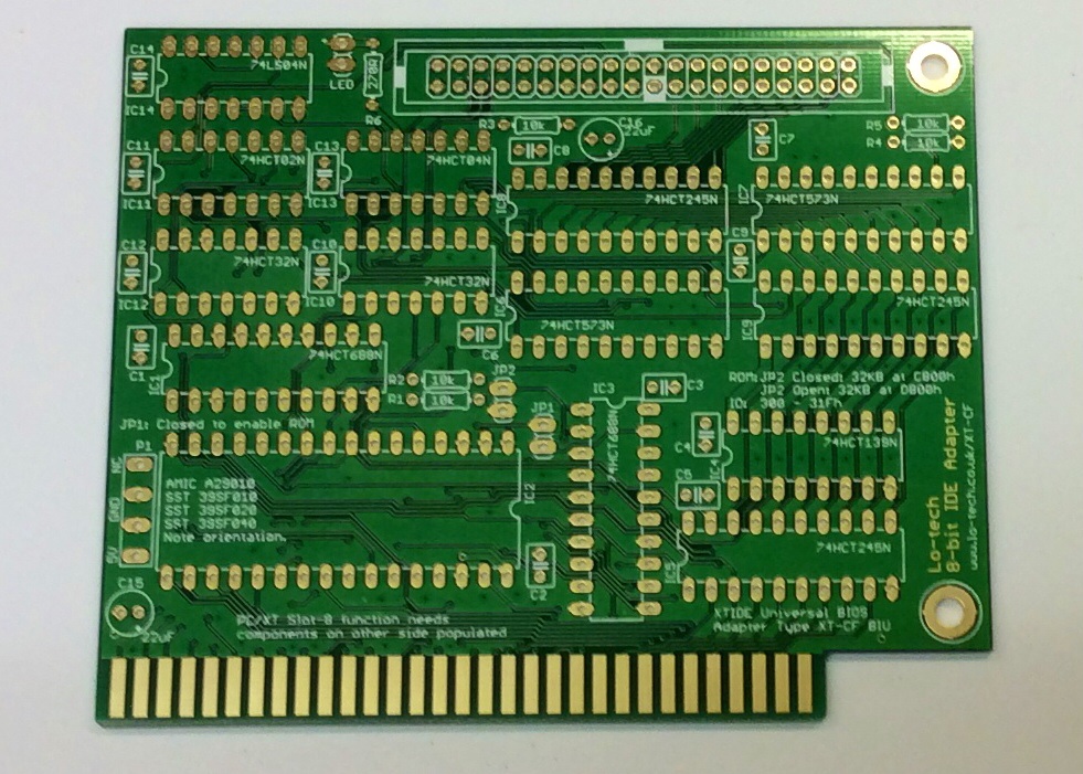
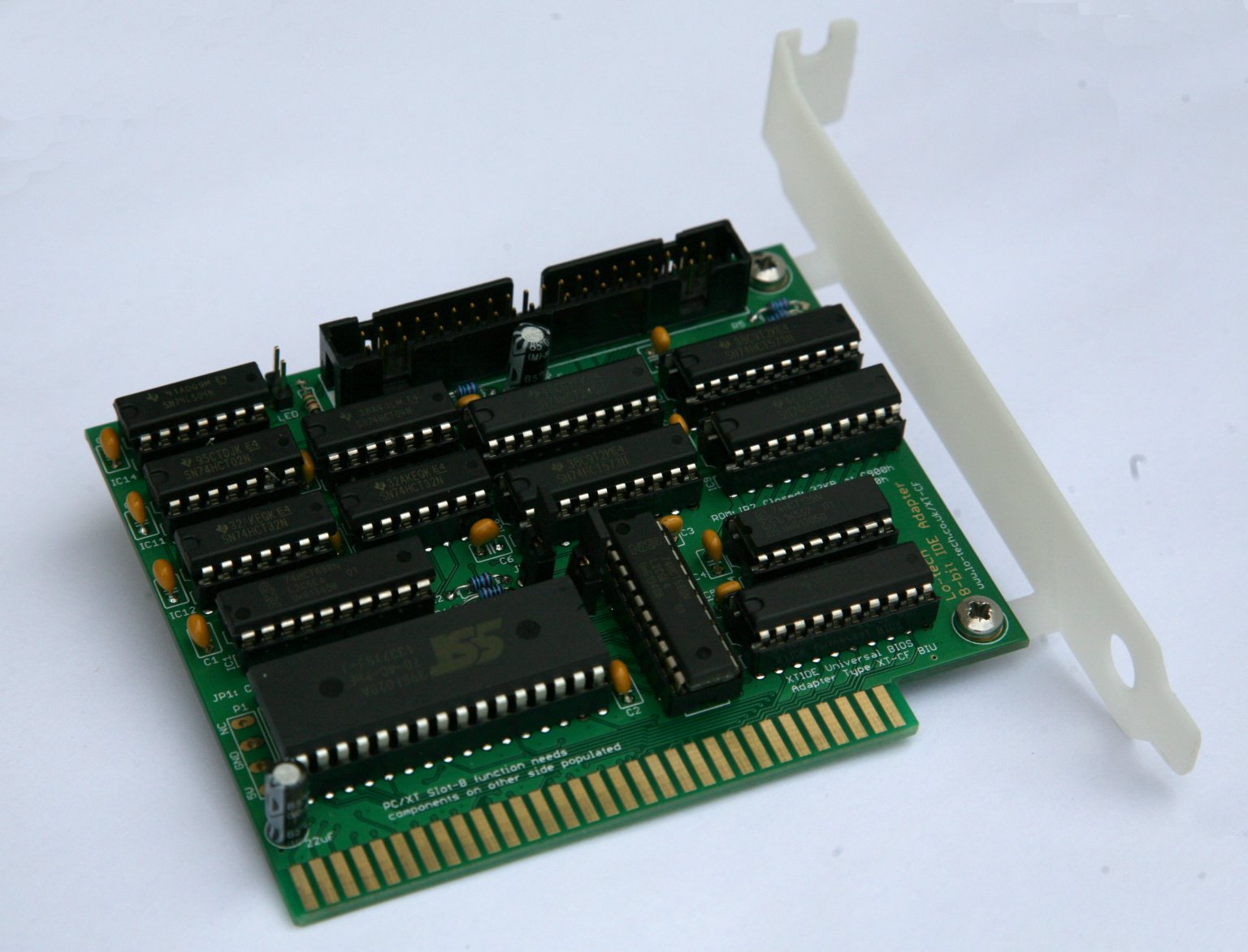
The Lo-tech 8-bit IDE Adapter is a bootable IDE controller for vintage PCs with only 8-bit ISA slots – basically PC/XT class hardware. The adapter is a development of the the Lo-tech ISA CompactFlash Adapter, adding an 8- to 16-bit MUX to make possible the use of normal hard drives, including current SATA drives (via an adapter like this). In this post, I’ll cover how to build the adapter and get it running.
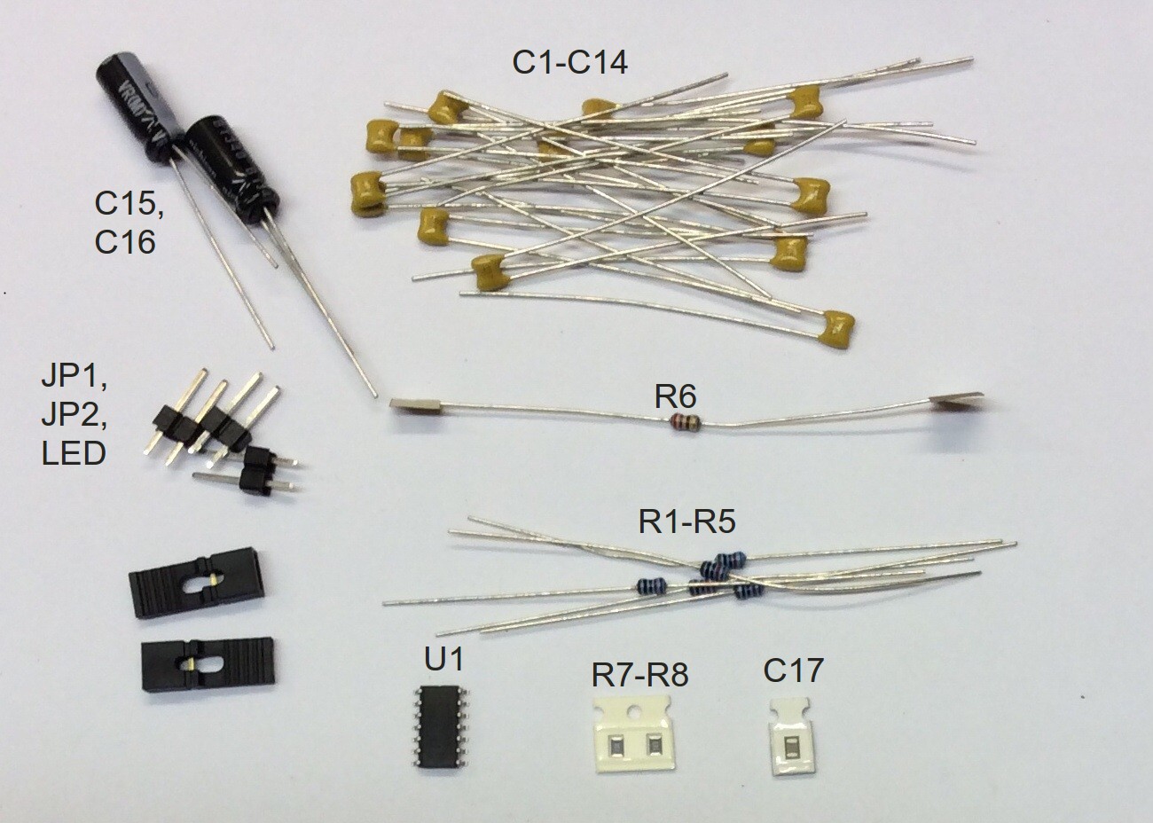
Components
Here’s what’s in the kit bag:
The only tricky parts are the SMT parts on the solder side of the board, basically a SOIC 74LS33D and a few resistors. These parts provide IBM PC/XT Slot-8 compatibility and enhanced read performance in PC/AT class systems, and can be simply left of if that functionality is not required.
The Build
Build order is basically determined by the height of the components, so that they’re held in place whilst soldering:
SMT components first, if these are being used
Resistors R1 to R6
Capacitors C1 to C14
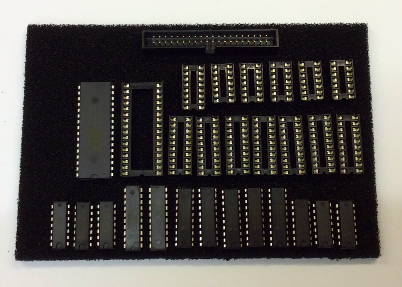
IC sockets. Check correct orientation (the notch should line up with the notch shown on the board silkscreen). Solder one pin of each first, then check the sockets are properly against the board. Once two or more pins are soldered, they will be very difficult to remove.
2-pin headers JP1, JP2, LED. As with the sockets, solder one pin first and then check alignment.
40-pin header HD1. First remove the key pin from the header using some small pliers unless key-pin provided 5V power is required (for example, to power a directly connected SATA converter). Again, solder one pin and then check alignment. Work quickly on each pin to avoid overheating the header plastic, otherwise the pins can become misaligned.
At this point the board will have a lot of flux residue that needs to be thoroughly cleaned off:
The board can be cleaned by immersion in either warm de-ionised water, isopropynol, or a specific flux remover and gentle agitation with either a toothbrush or an ultrasonic cleaner. Once satisfactorily cleaned, the two electrolytic capacitors C15 and C16 should be added, and the respective soldering areas cleaned again.
Once cleaned, check the joints thoroughly for any dry-joints or bridges (shorts), particularly around the SMT components (if fitted).
Finishing the Board
With the soldering done all that’s left to do is to dry thoroughly, for example with warm air (i.e. a hair dryer), add the ICs and slot bracket, then flash the BIOS.
Before the ICs can be fitted to the sockets, the pins need to be aligned using an alignment tool like this (ICs provided in Lo-tech kits are shipped ready aligned).
Errata
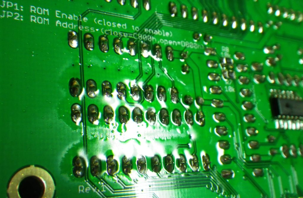
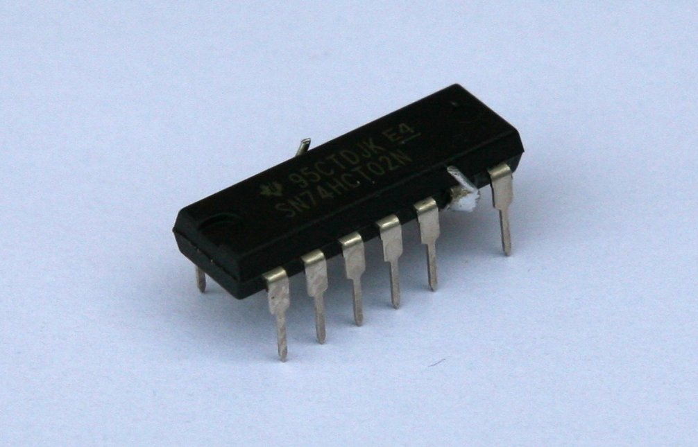
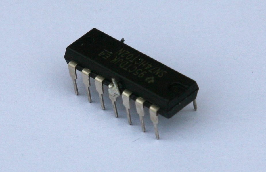
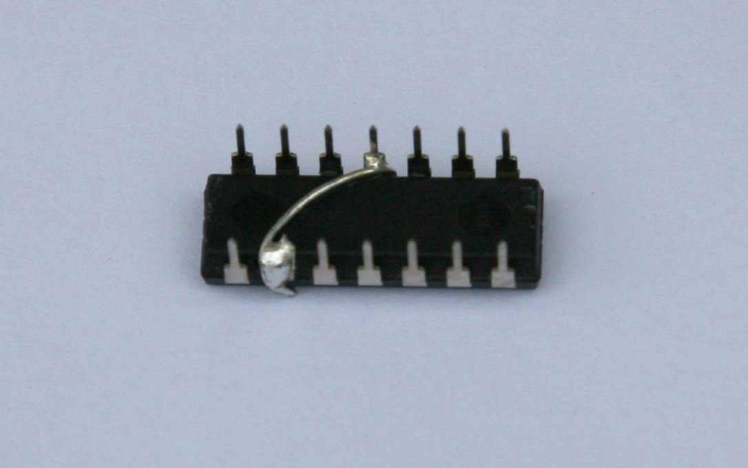
The first version of this board contains one error, which can be fixed by modifying the 74HCT02N that will be fitted as IC11 – pin 6 should be jumpered to pin 11, and pin 6 clipped or bent so it doesn’t make contact with the DIP socket. Here’s what the mod looks like (click on the images for a larger view) with the off-cut from a resistor used to make the connection:
Without this modification, the write latch load signal is masked unless the request is port 0, which works for the data register but also means no commands can be issued to the drive! Instead, the signal should be masked only when the request is port 1, which as it happens is on pin 11 already. Note that this modification applies only to the first revision boards; no modifications are required for the Rev.2 board.
Mounting the Chips
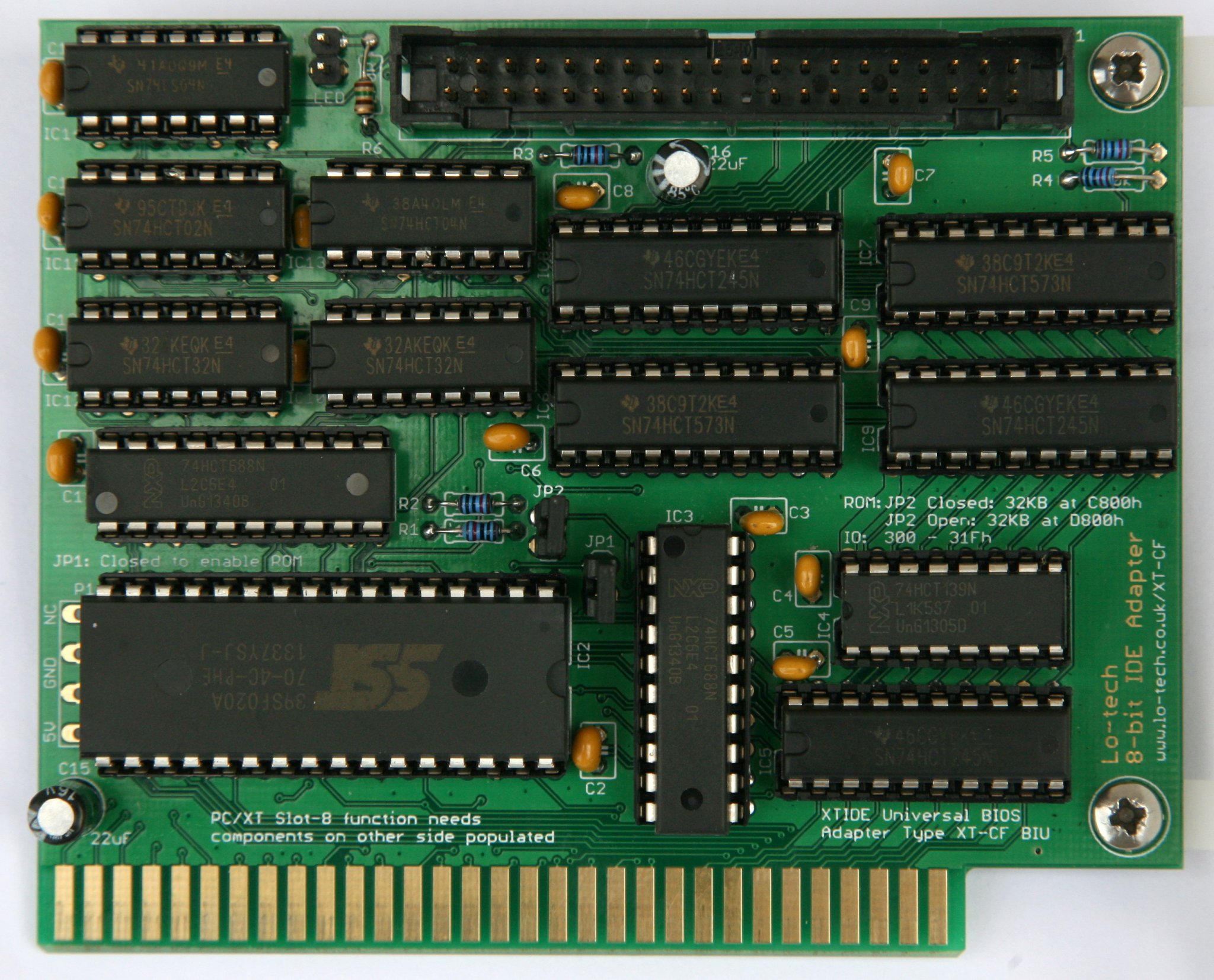
Once the pins are aligned, the chips can be mounted in the sockets, Ensure the chips are fitted in the correct orientation, shown by the notches. Here’s a finished board, for reference:
Flashing the BIOS and Testing
Once assembled and fitted in a PC, the BIOS needs to be stored in the flash chip on the card. There’s no external EPROM programmer needed – the chip can be flashed directly from DOS in the machine, using the Lo-tech FLASH utility.
Depending on how JP2 is set, the command needed is either (assuming the ROM image from the wiki is being used):
A:\>flash 8bit-ide.bin c800
or
A:\>flash 8bit-ide.bin d800
Once this has been done, reboot the PC and the XTIDE Universal BIOS should be displayed after the system POST, and any connected hard disks detected.
To get the machine to boot from the adapter, the primary disk will need to be partitioned (a primary and active partition created, using DOS FDISK utility) and then formatted (FORMAT C: /S). If the disk has been used with a newer operating system (anything other than DOS), a new Master Boot Record is probably needed as well, which can be created using DOS 6.22 by running FDISK /MBR.
PCB and Kit Availability
Rev.1 PCBs and kits are available in the store now – note these need one of the 74HCT02 chips modified as detailed above as part of the assembly process.
Lo-tech is in no way associated with the sellers of products on other sites linked to on this page (which are provided to provide an example of the types of products available).
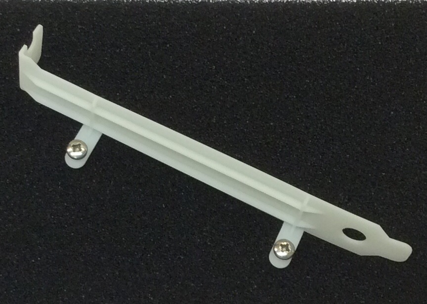
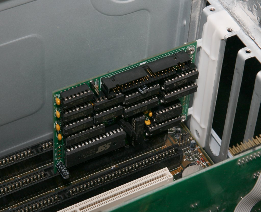
My first attempt at an ISA slot bracket produced on a 3D printer (see here) went reasonably well, with the result perfectly able to do the job of supporting the cards in the slot. But they were a bit more bendy that I’d hoped, so here is a revision 2 with ribs running down the length and either side of the card mounting fingers:
These have again been printed with a high definition SLA process and are much less flexible than the first version. These look good installed and do the job of holding the cards upright perfectly:
The Lo-tech 8-bit IDE Adapter is a bootable IDE controller for vintage PCs with only 8-bit ISA slots – basically PC/XT class hardware. The adapter is a development of the the Lo-tech ISA CompactFlash Adapter, adding an 8- to 16-bit MUX to make possible the use of normal hard drives, including current SATA drives (via an adapter like this). In this post, I’ll cover how the adapter works.
16- to 8-bit MUX Design
The main design goal with this adapter is to enable the use of standard, 16-bit drives (‘ATA drives’) with PC/XT class hardware. ATA drives all use both 8- and 16-bit data transfers:
Port 0 – 16-bit data port. This is where the actual sector data is transferred
Port 1 to 7 – 8-bit command ports. This is how the drive is told what to do next, like read or write to a sector.
Port IO with 8-bit ISA Cards
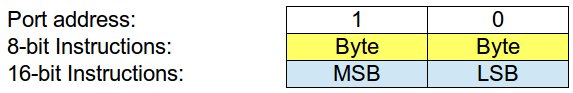
In the IBM PC, port IO can also be either 8- or 16-bit, even in XT class hardware with 8-bit ISA slots. Logic in the system known as the bus interface unit (BIU) makes this possible by breaking 16-bit instructions into two consecutive 8-bit bus cycles at consecutive 8-bit port addresses. Hence a single 16-bit port IO is, with 8-bit ISA cards, exactly equivalent to two consecutive 8-bit port IOs:
8-bit ISA cards can still use 16-bit CPU instructions (MSB=most significant byte, LSB=least significant byte)
Note that this applies specifically to hardware in 8-bit ISA slots; when a 16-bit instruction is used with a 16-bit device, all 16-bits are transferred in one bus cycle (and via a single, port 0 in this example). This difference provides both a problem and an opportunity – the ATA specification defines port 0 (only) for (the 16-bit) data transfer, so it just won’t work ‘as-is’ via an 8-bit slot, but secondly the CPU and BIU will already deal with one half of the equation. The 8-bit adapter just needs to break apart 16-bit drive IO into two ISA bus cycles, without the drive noticing.
Port Remapping
Making ports 0 and 1 free for the ATA data register is straightforward – just shift all the command addresses left one bit, a trick already used in the XT-CF line of adapters. With the BIOS code similarly updated, it makes no difference to the drive and this then means address line A0, which distinguishes port 0 from port 1, is free for the adapter to use for something else.
With that in place, 8- or 16-bit port IO can be performed to any of the drives registers, though the ATA specification only calls for 16-bit IO on the data register.
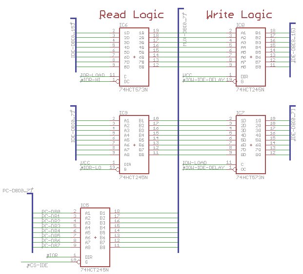
The MUX
The 8- to 16-bit MUX itself uses a separate 74HCT573 and 74HCT245 pair for reads and writes, and another 74HCT245 to link back to the PC data bus. The ‘573 is a latch (like a one-byte memory) providing temporary storage, and the ‘245’s are buffers that can be switched on at will, enabling isolation of certain signals when required.
For reads:
First bus cycle: a 16-bit word is transferred from the drive. The LSB is presented to the PC data bus and the MSB stored in a latch.
Second bus cycle: data from the latch is presented to the PC data bus, and the IO signal to the drive suppressed.
For writes:
First bus cycle: LSB presented on the PC data bus is stored in the latch, and the IO signal to the drive suppressed.
Second bus cycle: MSB presented on the PC data bus is presented to the drive interface MSB, and data from the latch is presented to the drive LSB.
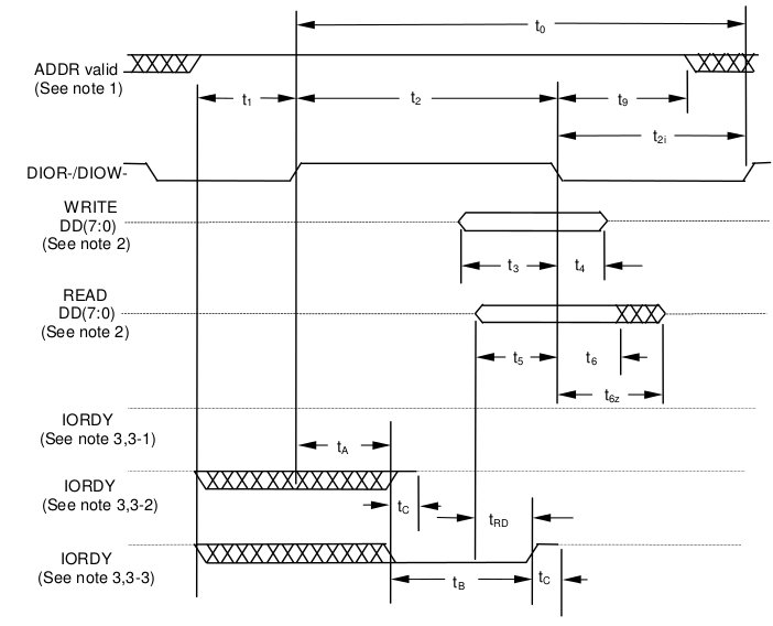
Interface Timing
The timing of this process needs some consideration as we need to be sure that data is stored in the appropriate latch before it disappears from the data bus, and secondly that data is presented until just after whatever is receiving it has stored it – this is measured as the data hold time.
ATA Interface Timing Diagram
For ATA mode 0, the specified data hold times are 5ns for reads (t6), and 30ns for writes (t4).
For writes, to keep data presented after DIOW line is released at the drive, the latch and buffer outputs are fed from the delayed signal (*IOW-IDE-DELAY in the schematic)
For reads, the hold time specification of the ‘HCT573 must be observed (9ns). The data being presented by the drive is held beyond the latch time since the drive DIOR line is fed from the delayed signal.
The delays are made by feeding the respective signals through three NOT gates (the control logic already inverts it once) in IC14. The delay can be controlled by the component choice (~15ns with SN74LS04N, or about 25ns with SN74HCT04N). Without the delay lines, for example in the case of a write the latch output would be turned off just as the drive latches the data because of zero hold time – the data may or may not still be valid as the drive stores the data.
PCB Errata
In the first version of this board, the write latch load signal is masked unless the request is port 0, which works for the data register but also means no commands can be issued to the drive! Instead, the signal should be masked only when the request is port 1, which can be fixed by modifying the 74HCT02N that will be fitted as IC11 – more details to follow in a build post.
Lo-tech is in no way associated with the sellers of products on other sites linked to on this page (which are provided to provide an example of the types of products available).
The lo-tech ISA CompactFlash adapter continues to be the top selling lo-tech project kit, providing a bootable fixed disk option for vintage PCs with the added satisfaction of being something that can made by the hobbyest. But one question just keeps coming… can it be used with a real hard disk?
The answer is yes, but only ATA-2 disks (typically 80 to 250MB and obviously now long past their use-by date) as it depends on ATA-2 8-bit transfer mode, which of course is still supported by all CompactFlash cards. This makes it relatively simple and small enough for the Sinclair PC200 that was the design motivation. The 40-pin IDE header just avoids fiddly surface-mount CompactFlash headers – adapters are available on eBay very cheaply (random product link).
So to answer the continuing demand for an adapter compatible with all normal IDE drives, I’ve taken the ISA CompactFlash adapter design and added the 16- to 8-bit logic (the MUX) to make it work with normal drives – including SATA drives and SD cards via appropriate adapters (random links: sata adapter, SD adapter). This has doubled the PCB size and increased the chip count from 6 to 15, but here it is!
The Lo-tech 8-bit IDE Adapter is an IDE controller for 8-bit ISA slots that works with normal IDE and SATA drives
Adapter In Action
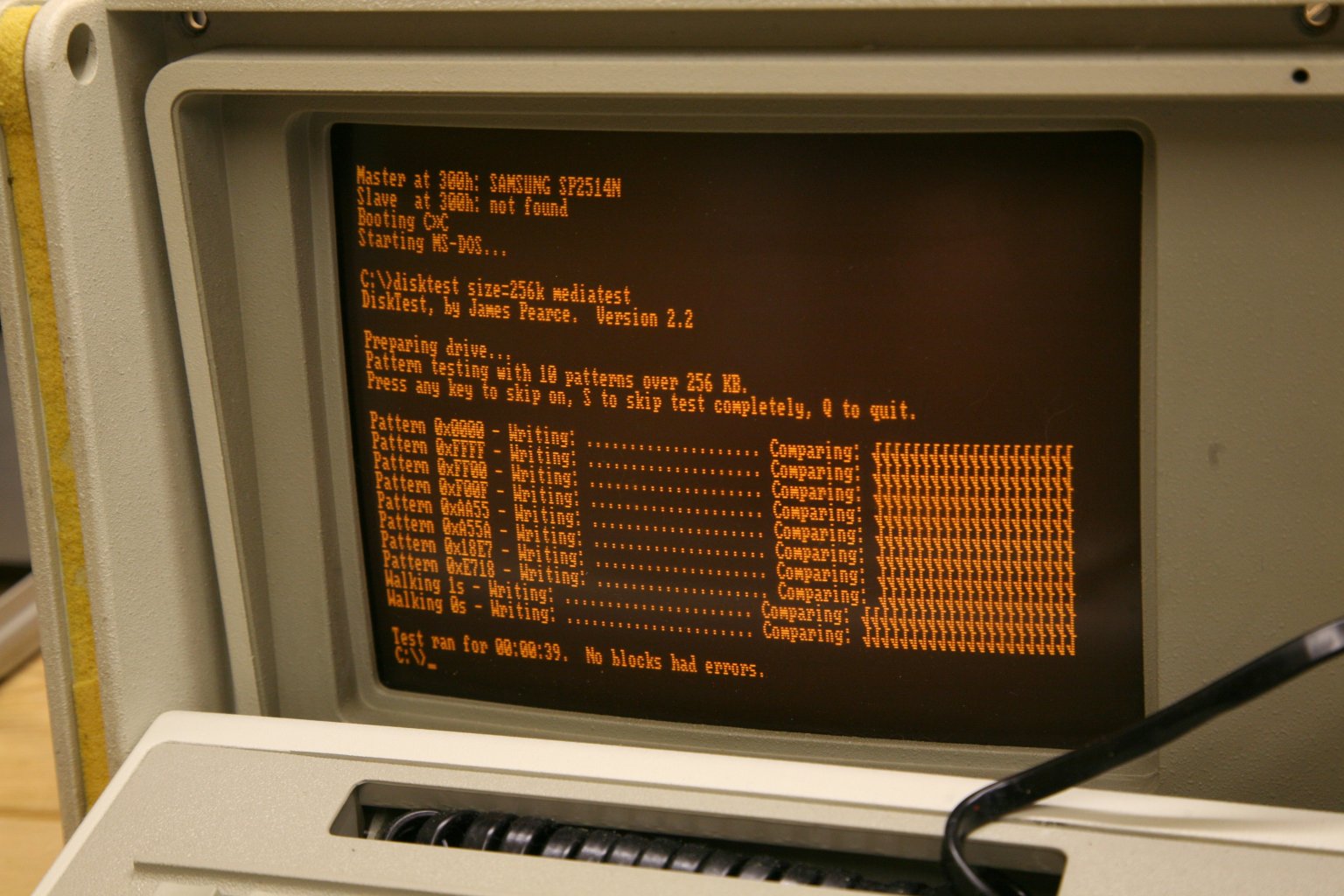
The detail of how the adapter works I’ll cover in another post, but for now here is an IBM PC 5155 booting up from it and running some pattern tests:
Testing so far is limited, but all drives tested have worked, including two SATA drives. Performance wise, it runs at about 250KB/s with a 4.77MHz 8088, and I’d expect about 400KB/s with a V20 (thanks to the REP INSW optimisation).
More details, and PCBs, coming soon!
Lo-tech is in no way associated with the sellers of products on other sites linked to on this page (which are provided to provide an example of the types of products available).
This website uses cookies to improve your experience. We'll assume you're ok with this, but you can opt-out if you wish.AcceptRead More
Privacy & Cookies Policy
Privacy Overview
This website uses cookies to improve your experience while you navigate through the website. Out of these, the cookies that are categorized as necessary are stored on your browser as they are essential for the working of basic functionalities of the website. We also use third-party cookies that help us analyze and understand how you use this website. These cookies will be stored in your browser only with your consent. You also have the option to opt-out of these cookies. But opting out of some of these cookies may affect your browsing experience.
Necessary cookies are absolutely essential for the website to function properly. This category only includes cookies that ensures basic functionalities and security features of the website. These cookies do not store any personal information.
Any cookies that may not be particularly necessary for the website to function and is used specifically to collect user personal data via analytics, ads, other embedded contents are termed as non-necessary cookies. It is mandatory to procure user consent prior to running these cookies on your website.
Lo-tech products are sold via TexElec. Please visit their web site texelec.com. Dismiss