Archives for james

Shugart and the Bubble

intel-bubble-logo-1981-banner

Magnetic Bubble Memory (MBM) was positioned as a major contender for computer storage in the late 1970s, even appearing in popular culture when at the center of the plot in Knight of the Phoenix.  The technology seemed to offer everything flash offers today, and is the basis of some surprising patents such as this iPod forerunner filed in 1979.

The TMS 9916 Bubble Memory Controller datasheet surmised,

…the main advantages are the low entry price versus disks…, nonvolatility…, and high-density storage… ideally suited for portable applications as well as providing memory for traditional processing systems

What Is Bubble Memory?

One_bubble_memory_track_and_loop

Bubble memory works like a shift register

MBM works by storing bits as cylindrical magnetic domains (the bubbles) on a film mounted within an electromagnet array, which is used to move the bubbles through the film.  Functionally, MBM is like a massive shift register – moving the bubbles results in one (stored) bit being read from one end, and a new bit being supplied at the other.

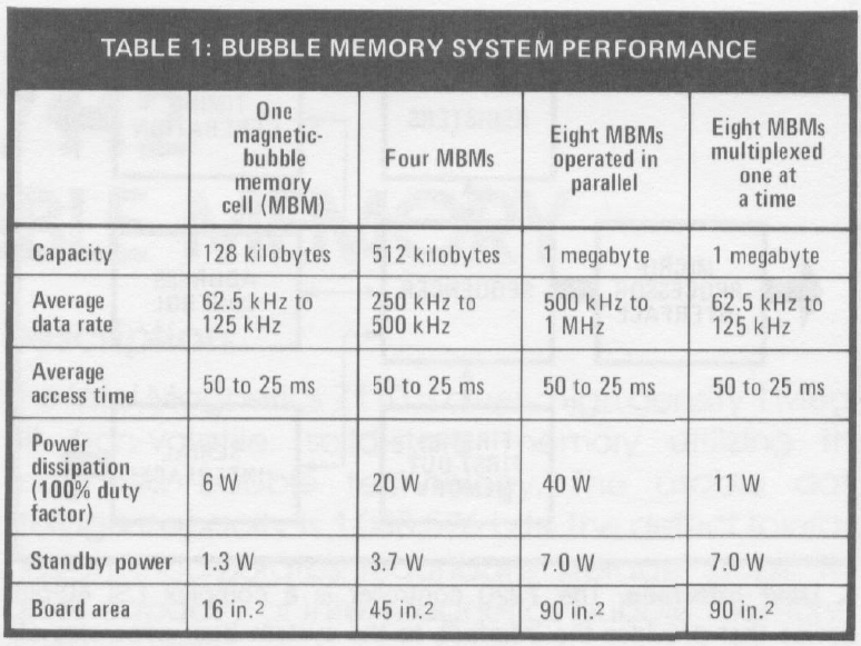
By the end of the 1970s, practically every major semiconductor manufacturer was working furiously on this technology, and of course Intel was no exception with its subsidiary ‘Intel Magnetics’.  Their 1979 Design Handbook for the Intel Magnetics One Megabit Bubble Memory is well worth a look, and includes a technical article as an appendix with some performance specifications.  The power consumption jumps out as surprisingly high for a solid-state technology.

Conner & Shugart

st-506-drive

ST-506 (image: fosketts.net)

Meanwhile Finis Conner and Al Shugart, having enjoyed some success as Shugart Associates with 8″ floppy and fixed disks, in 1979 formed a startup to produce 5.25″ fixed disks for the emerging personal computer industry.  Shugart Technology was born, named deliberately in the expectation of some free publicity from Shugart Associates owner Xerox.

Less than a year after incorporation, they led the storage industry with the introduction of the micro-Winchester ST-506, the first 5.25″ form factor hard drive.  With 5 MB usable capacity, it immediately provided a problem for bubble technology – and DEC (absorbed by Compaq in 1998) provided Shugart with their first major order, ST-506 drives being destined for its Rainbow PC in a deal apparently negotiated over cocktails and written on a napkin (source).

Disk vs Bubble

intel-imb-100-development-board

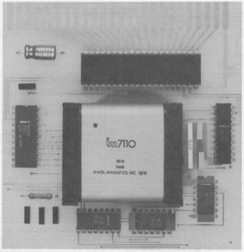
Intel IMB-100 Development Board

The limitations of MBM were, by 1980, becoming clear.  Whilst requiring complex controller logic similar to that of a hard disk, it was power hungry and slow in comparison: Intel’s iSBC254 bubble memory storage board needed 32W per ½MB, had a 48ms access time, burst data rate of 48KB/s and a physical volume of 50cu.in.

In contrast, the ST-506 drive boasted 10x the capacity in a package about 3x the volume, had 10x the burst data rate, and needed less than a tenth of the power per KB.  The death-knell for bubble though came when, setting the pace of capacity expansion we’ve expected since, what was by then Seagate produced the 10MB ST-412 in 1981.

Originally to be named ST-512, the drive heads were changed to thin-film type and name updated to ST-412 according to a comment on theregister, but either way the significance in vintage computing is simple: it was selected by IBM for it’s PC/XT 5160 (produced from 1983 to 1987), putting Seagate on track to become one of the most successful storage vendors today.

Meanwhile with bubble further compounded by poor yields and the need for gadolinium gallium garnet and highly toxic chemicals, by the early 1980s pretty much all efforts with bubble memory had been dropped.

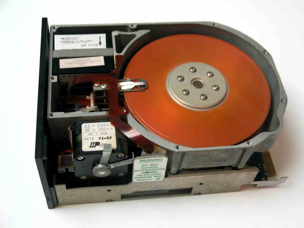
ST-506/ST-412 Reliability

Even as of 2013, there’s no shortage of working ST-412 drives – I acquired one recently in an IBM PC/XT, which when powered on presumably for the first time in about 20 years booted up straight-off, loading the school accounts system it still stored without a fuss.

Running a low-level format (using the IBM XT Diagnostics disk – the formatter is hidden away in the diagnostics menu under fixed disk tests) gives a good indication of the state of a drive, and it completed without even the hint of a bad sector.  Not bad for a 28-year old drive, especially one whose “magnetic disks have a life expectancy of 5 years” according to the service manual.

Performance

The ST506 interface used by the ST-506 and ST-412 drives was derived from the SA1000 MFM floppy interface Shugart designed in the mid 1970s, and in the PC/XT it provided 5Mbps and 17 sectors per track.  Raw transfer rate is therefore about 600KB/s, but in practice much lower because an interleave was needed to allow the CPU time to collect sector data.  Running my simple disk test utility the disk does about 68KB/s with the default 6:1 interleave.

Bubble Today

Bubble memory has popped up again more recently – MIT proposed a microfluidic bubble memory in 2007 (ultimately too slow) and IBM has been working on racetrack memory for some time.  Whilst (as of 2013) it seems unlikely that bubble will be back any time soon, IBM Research suggests that Storage Class Memory (i.e. racetrack) could become mainstream if work on 3D NAND Flash fails to deliver.

Sinclair PC200 XT-CF Card

sinclair-pc200-banner

A few weeks back I wrote about the lo-tech ISA CompactFlash Adapter designed to fit the Sinclair PC200, at the request of a system owner, and based on a few ideas I already had on the drawing board at the time.

Being simple to make and cheap, the adapter has found a home in many machines besides the Sinclair already – only a couple of PCBs are left and the feedback from assemblers has been good.

sinclair-pc200-with-lo-tech-isa-compactflash-adapter-fittedThe main challenge with the Sinclair is the available expansion slot height, which is what the small form-factor adapter was designed to solve.  Here it is fitted to the Sinclair, with the top cover fitted.

Since the Sinclair doesn’t have any spare power connectors, make use of the 4-hole power outlet on the PCB to attach a floppy-drive style power lead to power an IDE to CompactFlash adapter (alternatively the keypin on the adapter will supply 5V, if the CompactFlash adapter in use supports this).

xtidecfg-ide-controllers-settingTesting, after a couple of false starts, has been successful so far.  Be sure to set ‘IDE Controllers’ to 1 (and the adapter type to XT-CF of course) when configuring the XTIDE Universal BIOS.  The BIOS can be written out using the lo-tech XT-CF flash utility.

XT-CF Card for Tandy 1400 Series Laptops

tandy-1400-banner

Tandy helpfully included an expansion slot in their 1400 series of laptops, and in places there is reference to an expansion box, but it seems it never made it to market.  The later 1400FD and 1400HD models retained the expansion slot and added a second (slightly different) slot for an MFM HDD controller, as implemented in the 1400HD.

The expansion slot is basically an 8-bit ISA slot, but with a different pinout and a few differences, in a custom card form factor to fit in the machine.  Power budget is also limited to 200mA, according to the service manual.  Fortunately, Tandy documentation provides everything needed to create a card – so here is what I believe to be the first ever expansion card for Tandy 1400 Series laptops (only about 20 years late):

CompactFlash-Adapter-for-Tandy-1400-Series-Laptops-assembled

Expansion Card Design

Based on the information available in the Tandy technical reference, I’ve created a wiki page detailing everything about the expansion slots.  Some of the Tandy documentation is contradictory, but my wiki is based on what is now a proven design.  I’ve also included an Eagle layout for the PCB (restricted to a 100 x 100mm footprint, to enable low-cost manufacture by SeeedStudio).

XT-CF

My XT-CF cards provide hard disk functionality to PC/XT and PC/AT class machines based on CompactFlash (or microdrives), and for the Tandy 1400 the design needs just four ICs – a flash ROM, two 74688 address decoders and a 74139 decoder.  Being XT-CF compatible, the design is fully supported by the XTIDE Universal BIOS (from build r554).

BIOS Initialisation

I built this board a while back, and although BIOS flashing went OK the machine didn’t want to initialise the XTIDE Universal BIOS.  The BIOS was clearly detecting the option ROM as the floppy seek test was performed on only the first floppy with it present (the BIOS assuming that an HDD would be installed in place of the second floppy, exactly as the 1400HD was shipped), but the BIOS initialisation messages never appeared.

This has had me stumped and the board simply sat on the side since.  But recently XTIDE Universal BIOS project lead Tomi posted a code update (in r552):

XTIDE Universal BIOS can now be initialized if non-standard main BIOS does not call INT 19h or if INT 19h handler is replaced by some other BIOS.

And sure enough, the BIOS fired into life and the machine booted (and yes, the SuperTwist LCD screen really does look this bad):

tandy-1400-xt-cf-boot

The solution isn’t quite perfect – the fixed disk is inaccessible when restarted via CTRL-ALT-DELETE, but since boot time on this machine is identical for both soft boot and cold boot, this is just something that we need to live with for now.

1400LT, 1400FD and 1400HD

For 1400FD systems at least with BIOS 1.04, the system BIOS assumes the second floppy isn’t installed when the XT-CF option ROM is present (this may also affect 1400LT systems).  For now this is a limitation, but with 32KB of flash ROM available it should be possible to resolve it by adding a floppy BIOS to the card.

For 1400HD machines, the MFM controller must be removed since both cards have their BIOS at C800h (upper memory space is somewhat limited in the 1400 series as Tandy included RAM in the upper memory area for use as a RAM disk).

Performance

Using the ‘XTplus’ XTIDE Universal BIOS build (thanks to the V20 CPU), DOS throughput (as measured with my own test utility) is at least 550KB/s.  Due to the 8-bit data bus and V20 microcode optimisations, there is no performance difference between standard 8-bit PIO and BIU offload modes (as set with XTCFMODE), although both modes are supported.

Availability

ENIG PCBs (gold plated) are available now through the shop page.

Components will also be needed from your local electronics outlet such as Farnell, Mouser or Digikey – full Bill of Materials in the wiki.  There is no bracket needed, since the card slides into the expansion slot guides within the system chassis, and the fit into the slot is tight enough not to need and further support.

8237 DMA Transfers Across Page Boundaries

IBM-Reference-Books-Banner

The 8237 DMA controller in the original PC/XT (and its clones) is fundamentally an 8-bit device with a 16-bit address space – perfectly matched to the MCS 85 family of which it was a part.  So to make it work with the 20-bit address space of the 8086 and 8088, IBM added a 4-bit ‘page register’ for each of its four DMA channels using a 74LS670 (a quad 4-bit register file).

The 8237 and the 74LS670 though are broadly independent; the page register does not automatically increment when the address register wraps around to zero.  This has two implications: normal segment:offset addresses must be converted to a linear, 20-bit physical address, and DMA transfers cannot cross a 64 KB page boundary.

Determining the Physical Buffer Address

segment-offset-to-linear-address-for-dma-controller

Code in the XTIDE Universal BIOS illustrates how to convert a standard segment:offset address (presented in ES:SI) to a linear address, with just the 8088 instruction set:

     xor        dx, dx      ; clear DX
     mov        ax, es      ; copy ES to AX
 %rep 4 
     shl        ax, 1       ; shift left 1, MSB into carry...
     rcl        dx, 1       ; ...and from carry to DX LSB
 %endrep                    ; repeat for the 4 MSB bits
                            ; AX now has ES SHL 4, and DX has ES SHR 12 
     add        si, ax      ; add AX to SI, to get low 16-bits in SI
     adc        dl, dh      ; if it overflowed, increment DX (DH is zero)
     mov        es, dx      ; and save DX back in ES

DX needs to end up with ES SHR 12 because IBM hooked up the 74LS670 DMA page register to the low four-bits of the data bus, so programming the high 4-bits of the physical address is achieved from the low 4-bits of a CPU register.  The addresses are then loaded into the DMA controller address register (in two halves, since the DMA controller has only an 8-bit data bus) and the associated page register.  In this example, the port addresses are for channel 3:

     out        0Ch, al                ; Reset flip-flop to low byte 
     mov        ax, es                 ; Get high 4 bits
     out        82h, al                ; Page register for Ch.3 
     mov        ax, si                 ; Get low 16 bits
     out        06h, al                ; Send low byte to Ch.3 address register
     mov        al, ah                 ; 
     out        06h, al                ; Send high byte to Ch.3 address register

Crossing a 64KB Boundary

Since the page register isn’t incremented by the DMA controller, a DMA transfer can run up to a page boundary at which point it (and the associated page register) must be re-programmed for another transfer into the next physical page.  Splitting a transfer across a boundary therefore requires a check of the transfer size against the possible number of bytes up to a page boundary.

The code that follows assumes the maximum total transfer size is less than 64KB so allows for either one or two DMA transfers.

    ; On entry - buffer is in ES:DI, CX has bytes to transfer
    ; First calculate bytes up to physical page boundary
    mov        ax, di 
    neg        ax                 ; 2s compliment

    ; if DI was zero, carry flag will be cleared (and set otherwise)
    ; When DI is zero only one transfer is required if total DMA
    ; transfer size is restricted to < 64KB
    jnc    .TransferDmaPageWithSizeInCX

    ; CF was set, so DI != 0 and we might need one or two transfers
    cmp        cx, ax                    ; if won't cross physical page boundary... 
    jbe    .TransferDmaPageWithSizeInCX  ; ...perform transfer in one operation 

    ; Calculate how much we can transfer on first and second rounds 
    xchg        cx, ax            ; CX = BYTEs for first page 
    sub         ax, cx            ; AX = BYTEs for second page 
    push        ax                ; Save bytes for second transfer on stack 

    ; Transfer first DMA page 
    call    StartDMAtransfer 
    pop         cx                ; Pop size for second DMA page 

.TransferDmaPageWithSizeInCX: 
    ; Fall to StartDMAtransfer 

StartDMAtransfer:
    ; DMA controller programming and transfer is completed here
    ; This code will be hardware dependent
    ; ...

    ; Once transfer is done, update physical address in ES:DI
    ; since IO might need several calls through this function
    ; (if crossing a physical page boundary)
    mov        ax, es             ; copy physical page address to ax 
    add        di, cx             ; add requested bytes to di 
    adc        al, 0              ; increment physical page address, if required 
    mov        es, ax             ; and save it back in es 

    ret

Purpose

The DMA controller in the original IBM PC really has a few reasons for being – RAM refresh of course, background transfers (as used by SoundBlaster sampled audio for example), and high-performance transfers.  The 8237 DMA controller is usually noted for its lack of performance, but that perception came about because CPU speed soon eclipsed it.

Operating in a 4.77MHz 8088, the DMA controller is the only way to transfer data to or from a peripheral in consecutive, back-to-back full-speed bus cycles (in later PCs, the DMA controller is throttled to about 5MHz to ensure peripheral compatibility).  Of course it’s made more difficult by the boundary crossing issues and requirement to pause for RAM refresh, but the controller can provide the fastest possible transfers as demonstrated by my XT-CFv3 DMA Transfer Mode.

Lo-tech ISA CompactFlash Board

Another PCB 🙂

Lo-tech ISA CompactFlash Adapter

I was contacted recently by the owner of a Sinclair PC200 (an XT class machine in an Atari ST style case) about my XT-CF boards, wondering if a custom board could be built for the machine, with its physical 50mm height restriction on its two ISA slots.  The quick answer to that is no, since the CompactFlash header is too big in either orientation, but I’d already been pondering on the idea of a super-simple PCB providing a 40-pin IDE header, based on the lo-tech 8-bit ROM board, so this seemed like a good opportunity to finish the design.

Lo-tech ISA CompactFlash Board: What is it?

A through-hole, small form factor 8-bit ISA adapter providing a 40-pin IDE header suitable for connection to a separate IDE to CompactFlash adapter (available cheaply on eBay).  By using a 40-pin header instead of a CompactFlash socket, home assembly of the device is made simple as all required components are 2.54mm pitch through-hole.

Other than the small form factor (and without any provision for a slot bracket), the PCB is a standard ISA card and can be used in any PC with an ISA slot.

New IDE Logic Implementation

Making an XT/IDE derivative in such a small PCB meant minimising the component count:

  • Whilst the XT-CF-lite was based closely on the original XT/IDE adapter, borrowing directly its OR and inverter gate design to provide IDE register access and IDE reset, with this new board this has been condensed into a single 74LS139.
  • Because of the 40-pin potentially cabled connection to the CompactFlash adapter, a buffer (74HCT245) is required, but with only 8-bit transfer mode supported (hence the CompactFlash designation), a 16-to-8-bit MUX isn’t required

Any CompactFlash or microdrive device should work with this adapter, and probably ATA-2 compliant hard drives (since 8-bit transfer mode is a requirement of ATA-2).

Extended Functionality

I wanted to include as much functionality as possible, so implementing the logic for IBM PC/XT Slot-8 compatibility (developed with the CPLD based XT-CF adapters) was a goal.  Although out of space on the ISA component side, the layout could accommodate a few SMT components on the ISA solder side: these are entirely optional, but when populated provide LED drive and Slot-8 functions.

The logic required to provide slot-8 functionality is straight-forward – it’s just an echo of MEMR or IOR when either the ROM or IDE ports (respectively) are selected, with an open-collector drive since other logic on the system board can also drive this signal (as I’ve written about before).  In this new board, this is implemented with a single 74LS33D quad NOR gate, the one spare gate being used to provide LED drive too:

Lo-tech ISA CompactFlash Adapter SMT Logic

LED drive requires the SMT 74LS33D populated since CompactFlash devices provide only minimal activity LED drive current, which is likely already absorbed by LEDs on the required CompactFlash to IDE adapter.

The boards are fully supported by the XTIDE Universal BIOS (from build R545), with standard 8-bit PIO transfer mode and the enhanced performance BIU Offload mode just as with the XT-CF-lite.  The DMA transfer mode of the XT-CFv3 is not however supported.

Availability

ENIG (gold plated) rev.2 PCBs are available via the shop page.

Components will also be needed from your local electronics outlet such as Farnell, Mouser or Digikey – full Bill of Materials in the wiki.

Understanding the IBM PC/XT 5160 Slot 8

IBM-Reference-Books-Banner

When IBM released the PC/XT 5160, the 8 ISA slots were a welcome improvement from the 5 in the original IBM PC 5150; multi-function cards weren’t yet common and the system board itself provided no IO capabilities other than the speaker and keyboard, so everything needed an expansion card.

Whilst seven of the slots operated just like those in the 5150, the slot nearest the CPU was special – the IBM Technical Reference noting Slot J8 is slightly different from the others in that any card placed in it is expected to respond with a ‘card selected’ signal whenever the card is selected, the key being a previously unused signal line B8:

CARD SLCTD (I) Card Selected: This line is activated by cards in expansion slot J8. It signals the system board that the card has been selected and that appropriate drivers on the system board should be directed to either read from, or write to, expansion slot J8. Connectors J1 through J8 are tied together at this pin, but the system board does not use their signal. This line should be driven by an open collector device.

By observation, B8 needs to be asserted (low) only when reading from a device in slot 8, which then sets the direction of the buffer U15 to transfer data from the XD bus (housing slot J8, the system ROMs and the DMA controller) to the D bus (slots 1 to 7).

Open Collector Drive

For novices like me, the last part of IBM’s text is important: the open collector drive (see evilmadscientist.com for a good description of this).  As other logic can drive B8, such as the ROM address decoder, a device driving ISA B8 can’t present a high-level drive when not asserted (the signal level is pulled up through RN1).  This can be achieved either directly using open-collector logic, or by using a separate buffer.

In my CPLD logic for the XT-CFv3, the logic looks like this:

 ISA-B8-CPLD-Logic

In the Lo-tech CompactFlash Adapter, I’ve gone with a separate buffer by distilling the logic down to some NOR gates, to minimise component count (the NOR gate also providing LED drive):

Lo-tech-CompactFlash-Adapter-ISA-B8-Logic

There’s probably a better way, but both of those work anyhow 🙂

Zero Wait State

The CARD SLCTD use for B8 was pretty much limited to the IBM PC/XT 5160 – the later PC/AT re-purposed the line as a “zero wait state” line, which has particular advantage for 8-bit cards.

As IBM started pushing the processor clock rates up, ISA at the time being effectively a local bus, IBM chose to limit the effective bus speed for 8-bit cards by adding wait states to achieve a bus cycle time of about 750ns, roughly equivalent to the 4.77MHz speed of the original PC.  At the time, expansion cards could be quite an investment so keeping things compatible was key.

Through the ZWS (B8) line in the PC/AT, and using the same basic logic as used to generate CARD SLCTD, the wait states can be eliminated for reads, and the logic simply extended to also consider IOW to also eliminate the wait states on writes.  This can boost throughput by 30% on a 6MHz AT, and 50% on a later 12MHz AT class machine.

More Information

XT-CFv3 DMA Transfer Mode

xt-cfv3-banner

The XT-CFv3 DMA transfer mode works in an unconventional way to deliver the highest possible throughput for the original IBM PC and PC/XT – here’s how.

The Intel 8237 DMA Controller

In the PC and PC/XT, the Intel 8237 DMA controller provides two functions – it keeps system memory alive by periodic refresh, and it enables transfers to and from IO devices with minimal CPU intervention (the floppy drive, many hard disk controllers, and SoundBlaster cards use DMA).  To achieve this, the DMA controller has four sets of DMA Request (DRQ) and DMA Acknowledge (DACK) lines and broadly, the process is:

  • DRQ is asserted by the requesting IO device (e.g. the floppy drive controller)
  • The DMA controller raises the HOLD line (connected to the 8088 CPU)
  • The 8088 CPU completes the current bus cycle, then asserts HLDA (Hold Acknowledge) so passing control to the DMA controller.  At this point, all output lines on the CPU are put in a high-Z state (effectively disconnected) and the CPU enters a waiting state
  • Now the DMA controller has control of the bus, it presents the memory address on the address bus and asserts AEN, which signals to IO devices not involved in the DMA transfer to disregard the bus cycle
  • The DMA controller next asserts DACK, preparing the IO device to present (or receive) data
  • Then the DMA controller asserts both IOR (IO read) and MEMW (memory write) concurrently, or IOW (IO write) and MEMR (memory read), so feeding data directly from the device to memory or vice-versa
  • The DMA controller transfer counter and memory address registers are then updated

What happens next depends on whether more data is available (so DRQ is still asserted), whether the transfer counter has reached zero, and finally the DMA controller operating mode.  In single byte transfer mode, the DMA controller will return control to the CPU by releasing HOLD after each byte, whilst in demand mode the process will continue until the IO device releases DRQ (block mode generally isn’t used because it can disrupt RAM refresh, as described below).

DMA vs Port IO

In demand mode DMA runs much faster than 8088/V20 transfers since with DMA, each byte is delivered to memory in just one bus cycle.  The 8088, on the other hand, has to read the byte from the IO device in one bus cycle then store it to memory in a second bus cycle, because both the IO device and memory use the same address bus.  On the 8088, the code to fetch a block of port mapped data is less than ideal:

mov cx, 512
 .TransferLoop:
 in al, dx
 stosb
 loop .TransferLoop

The instruction fetch and jumps of course make this slow, although it can be improved by unrolling.  In the XTIDE Universal BIOS, this is the basis of the 8-bit port-mapped IO operating mode for the XT-CF series, achieving about 170KB/s at 4.77MHz.  The V20 though streamlines this by eliminating instruction fetch and jump overhead:

mov cx, 512
 rep insb

Freeing up the bus for just the data by the elimination of all the instructions pays significant dividends – this delivers about 390KB/s at 4.77MHz (and is available in the ‘XTplus’ XTIDE Universal BIOS build, for V20/286 powered XT class hardware).

Making DMA Scream

DMA on the PC and PC/XT brings with it some challenges:

  • Programming the DMA controller absorbs many cycles
  • Control must be returned to the CPU every 15 µs (72 cycles) for RAM refresh
  • To play sampled SoundBlaster audio at 22KHz, the DMA controller must be available to service the SoundBlaster DRQ once every 216 cycles

For my goal of ultimate throughput, packing bytes back-to-back on the data bus is the key – and with each byte taking 4 cycles, 18 bytes can be transferred before disrupting RAM refresh.  For the XT-CFv3, this is achieved with some counter logic to release DRQ after 16 bytes (since that makes the maths easy and provides a margin of safety):

XT-CFv3-DMA-Counter-Logic

In the XT-CFv3, the oDRQ output in the schematic is delivered to the ISA bus via a 3-state output buffer, because the card must be able to co-exist with any original hard disk controller and DMA channels (DRQ/DACK pairs) can’t be shared as there are no pull-ups on the DRQ lines, so the card must drive the line continually when DMA function is in use.

Generating DRQ

Because DRQ is released by the counter, the DRQ lines on the IDE interface can’t be used – and in any case, DMA isn’t even supported by the majority of CompactFlash cards.  The XT-CFv3 therefore provides another mechanism – to allow the software direct control over DRQ through an IO port write (the address decoding for which appears in the schematic above as ‘XTCF_DRQ_PORT’).  This approach makes the transfer code itself elegant, once the DMA controller has been programmed:

mov cx, 32
 .TransferNextDmaBlock:
 out        dx, al                ; Raise XT-CFv3 DRQ & transfer 16 bytes
 loop    .TransferNextDmaBlock    ; loop also adds required wait-state

The results are heavily dependent on the media: the majority of CompactFlash cards support only single-sector transfers, and therefore the DMA controller must be programmed once for every 512 bytes transferred, which delivers about 420 KB/s – a vast improvement on 8-bit port IO.  But for devices supporting multi-sector transfers, performance rises to 530KB/s with an 8088 and a 560KB/s with a V20 (both at 4.77MHz).

More Information

Lo-tech XT-CFv3

Since working on the Dangerous Prototypes version of the XT/IDE project, I’ve been increasingly interested in ‘the storage problem’ for early 1980’s PCs – it’s both difficult to transfer files between machines and increasingly problematic storing data on them too, with still surviving hard drives now well into borrowed time.

My first attempt (the XT-CF board) was too limited to justify the assembly effort, and my second attempt (the XT-CFv2 board) pushed the 3.3V CPLD too far so suffering reliability issues.  Next I created the simpler XT-CF-lite, which Sergey has taken on and improved with his re-spin, using mostly through-hole components.

So the CPLD based project was apparently dead, until some 5V XC9536 CPLDs popped up again on Farnell (supply is sporadic but more are due): the XT-CFv3 board was born:

Lo-tech-xt-cfv3

The goal was to make a board with the DMA function of the XT-CFv2, but as easy to make as the XT-CF-lite (only the CompactFlash header represents something of a soldering challenge).  So the XT-CFv3 specs:

  • 8-bit ISA card providing bootable fixed-disk storage for PC/XT and PC/AT class hardware
  • Up to 8GB usable by MS-DOS (DOS limit)
  • CompactFlash header positioned to allow CompactFlash media to be exchanged through a custom ISA card slot, without opening the PC
  • 32KB in-system re-programmable flash ROM, providing storage for the XTIDE Universal BIOS boot ROM with 24KB free
  • Provides several transfer modes optimised for 8088, V20 and 286 machines
  • Up to 530KB/s in a stock PC/XT, and up to 1.1.MB/s in a 12MHz 286
  • Low-cost manufacturing requirements

Programmable Logic: the Xilinx XC9536

At the heart of the XT-CFv3 is the Xilinx XC9536 CPLD.  To me, these are little pieces of silicon magic – simply hook up the components on the PCB to the nearest convenient CPLD pin, then define in software the circuit logic the CPLD should perform and upload it into the CPLD.  This is great for home-brew projects like this, since once the basic PCB layout is done and the board electrically sound, the design can be revised over-and-over by just reprogramming the CPLD.

The XT-CFv3 logic is a greatly simplified version of that from the XT-CFv2, which aside from electrical reliability issues, was working well enough – so I was confident the logic would work.  Even so, six revisions were needed to finally bring the thing to life.  But it’s running now with three modes of operation – more on which will follow soon 🙂

DMA Transfers

DMA is the big XT-CFv3 feature: it offers performance way beyond what any disk controller ‘back in the day’ could do, achieving up to 530KB/s on a stock PC/XT.  The CPLD implementation makes this possible since it can do the work of many discrete logic chips (and of course be reprogrammed in the development phase getting it running).  More on this, and the other operating modes, to follow soon.

Availability

The XT-CFv3 is just entering field testing so is some way off still.  The plan though is to offer bare PCBs and brackets for home assembly.

In the mean time, Sergey has done a great job with his version of the XT-CF-lite, making it mostly through-hole so a little easier to make.

XT-CFv2 Shelved – What Happened?

XT-CFv2-Banner

The lo-tech XT-CF, itself really just a port of the Dangerous Prototypes XTIDEv2 board, worked well but it had become clear that by adding a few extra connections, the board could be made more flexible, and faster too.  There were a few unexplained CompactFlash media compatibility issues, but basically the board worked OK.  So enter the v2, much the same as the first board but able to work in IBM PC 5160 slot-8 use and run with DMA transfers (for up to 500KB/s in an XT).

With some prototypes made, once the logic and BIOS was switched to 8-bit transfers – eliminating the latch timing issue that has plagued all the XT/IDE derivatives – things seemed to be progressing well, so well that everything was in place to start an initial ‘public beta’ of fully assembled boards.

Reliability

When the idea of a 3.3V CPLD was first mused on at Dangerous Prototypes – because of the lack of availability of 5V parts – some queries were raised over quite how 5V tolerant the inputs would be in reality.  And it seems those fears weren’t without foundation, since steadily the prototype boards started to misbehave; they all seemed to follow the same pattern with DMA transfers going slow and then failing altogether, then memory-mapped IO failing next.  For whatever reason, basic port-mapped IO seemed to survive.

Stumped by this, I turned my attention to the XT-CF-lite board (now sold out, sorry!), keen to deliver ‘something’ after all this time.  And the board seems to work well – built on the 8-bit transfer mechanism and experiences with the XT-CFv2 in port-mapped mode, the board is entirely 5V 7400 series based, but critically there is no buffer on the data lines: the CompactFlash (or flash ROM) drive the data bus directly.  Which got me thinking.

Xilinx XC9536

Whilst the XT-CFv2 uses a tricky-to-solder 100-pin 72-macrocell CPLD, by eliminating all 16 CompactFlash data lines and the 8 ISA data lines, I wondered if the logic be moulded into an easier-to-handle VQ44 package CPLD?  I wanted to keep DMA and Slot-8 compatibility, but memory-mapped IO turned out to be something of distraction – it’s only faster because it enables 8088 CPUs to use REP MOVSB to make a transfer, but DMA is much faster on an 8088, and the V20 (and 286+) can use REP INSW anyway.  So losing memory-mapped transfers seems OK to me.

In a stroke of luck, I spotted forthcoming stock of Xilinx XC9536 CPLDs in VQ44 format at Farnell – absolutely ideal for this as the simplified logic easily fits in the 36 macrocells, and the 34 IO pins are just enough.

XT-CFv3

So round the prototype mill we go again, this project has turned out to be way harder and more time consuming than I was expecting 15-months back.  But it’s only a hobby and it is still progressing – I’m currently awaiting delivery of the first XT-CFv3 PCBs, although the CPLDs won’t be available until the end of February.  The logic is much simpler, the board will be easier to make like the Lite version.

In the mean time, I’m improving the flash utility to work with the cheaper and more readily available A29010 flash chips – so fingers crossed for 3rd-time lucky 🙂

Another PCB… the XT-CF-Lite

Beta testing of the XT-CFv2 has uncovered some compatibility and reliability issues that will take time to fix, so in the mean time – and conscious of the long development time already of these boards – I’ve turned my attention to making a simpler, more home-assembler friendly XT-CF derivative.

Surface-mount (SMT), especially the 0.5mm pitch components, seem to have put off home-assemblers, and then there’s the need to program the CPLD. Though SMT can’t be avoided because of the CompactFlash header, using SOIC chips but still in the same PCB footprint (and ISA slot bracket), things can be made a lot easier.

So the XT-CF-Lite – here it is!

What Is It?

Just like the XT-CFv2, it’s a self-contained ISA disk device, functionally like a hard-card, providing solid-state, bootable storage to any PC with an ISA slot – right back to the original IBM PC 5150.

What Gives?

This board provides the same basic functionality of the XT-CFv2 – a 32K (accessible) flash-based ROM (with 24KB available for any user purposes), XTIDE Universal BIOS support and the port-based IO transfer mode used by the XT-CFv2 by default. But there are some limitations, because the CPLD on the XT-CFv2 provides a wealth of logic space not present here, so the lite version misses out on BIOS port auto-detection, memory-mapped IO, DMA, slot-8 compatibility, and reduced-wait-state operation for PC/AT and above.

No Buffer?

Usually a buffer chip like the 74LS245 would be used between the ISA bus and the media, but I took a chance that one isn’t needed, because the CF card is directly connected (i.e. not cabled) and has 8mA output drive strength. And luckily, it seems to work!

That’s SMT – wasn’t is supposed to be easier to make?

We can’t get away from SMT and still use CompactFlash – through-hole sockets do exist on datasheets, but are near impossible to find. Compared to the XT-CFv2:

  • 0.5mm lead-pitch flash chip has been replaced with an easy through-hole DIP package, and the 100-pin CPLD has been eliminated altogether
  • 1206 package resistor networks have been replaced with a through-hole network
  • SMT 7400-series chips have 1.27mm lead-pitch and are pretty easy to solder

And of course there’s no CPLD programming to do once it’s assembled. The activity LED and driver IC (IC6) can be left-off if need be. The tiny 0603 package capacitors and resistors remain but are also quite easy. The hardest part is the CF header, but locating points on the header hold it in position whilst it’s soldered, and the trick is to use plenty of flux and flow solder over the pins generously, then use solder wick and more flux to clean up the job.

How Fast?

With the official XTIDE Universal BIOS, it will do about 150-180KB/s on a PC/XT. It’s possible to increase this about 20% by switching the BIOS to 16-bit IO cycles, but at the expense of system compatibility. 16-bit port IO is faster because it reduces the instruction count and off-loads some work to the bus interface unit (BIU), but in development of the XT-CFv2 it was found that some clones have errors in BIU logic resulting in byte-swapped data delivery.

Availability

PCBs and slot brackets are available now via the site Shop. Components can be found at Farnell, Digikey or Mouser. Full board details in the wiki.