
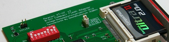
The lo-tech XT-CF, itself really just a port of the Dangerous Prototypes XTIDEv2 board, worked well but it had become clear that by adding a few extra connections, the board could be made more flexible, and faster too. There were a few unexplained CompactFlash media compatibility issues, but basically the board worked OK. So enter the v2, much the same as the first board but able to work in IBM PC 5160 slot-8 use and run with DMA transfers (for up to 500KB/s in an XT).
With some prototypes made, once the logic and BIOS was switched to 8-bit transfers – eliminating the latch timing issue that has plagued all the XT/IDE derivatives – things seemed to be progressing well, so well that everything was in place to start an initial ‘public beta’ of fully assembled boards.
Reliability
When the idea of a 3.3V CPLD was first mused on at Dangerous Prototypes – because of the lack of availability of 5V parts – some queries were raised over quite how 5V tolerant the inputs would be in reality. And it seems those fears weren’t without foundation, since steadily the prototype boards started to misbehave; they all seemed to follow the same pattern with DMA transfers going slow and then failing altogether, then memory-mapped IO failing next. For whatever reason, basic port-mapped IO seemed to survive.
Stumped by this, I turned my attention to the XT-CF-lite board (now sold out, sorry!), keen to deliver ‘something’ after all this time. And the board seems to work well – built on the 8-bit transfer mechanism and experiences with the XT-CFv2 in port-mapped mode, the board is entirely 5V 7400 series based, but critically there is no buffer on the data lines: the CompactFlash (or flash ROM) drive the data bus directly. Which got me thinking.
Xilinx XC9536
Whilst the XT-CFv2 uses a tricky-to-solder 100-pin 72-macrocell CPLD, by eliminating all 16 CompactFlash data lines and the 8 ISA data lines, I wondered if the logic be moulded into an easier-to-handle VQ44 package CPLD? I wanted to keep DMA and Slot-8 compatibility, but memory-mapped IO turned out to be something of distraction – it’s only faster because it enables 8088 CPUs to use REP MOVSB to make a transfer, but DMA is much faster on an 8088, and the V20 (and 286+) can use REP INSW anyway. So losing memory-mapped transfers seems OK to me.
In a stroke of luck, I spotted forthcoming stock of Xilinx XC9536 CPLDs in VQ44 format at Farnell – absolutely ideal for this as the simplified logic easily fits in the 36 macrocells, and the 34 IO pins are just enough.
XT-CFv3
So round the prototype mill we go again, this project has turned out to be way harder and more time consuming than I was expecting 15-months back. But it’s only a hobby and it is still progressing – I’m currently awaiting delivery of the first XT-CFv3 PCBs, although the CPLDs won’t be available until the end of February. The logic is much simpler, the board will be easier to make like the Lite version.
In the mean time, I’m improving the flash utility to work with the cheaper and more readily available A29010 flash chips – so fingers crossed for 3rd-time lucky 🙂
Social tagging: XT-IDE
So, did you ever end up making any of these? 🙂
Hi, the v2 board has been superceded by a v3 which uses a 5V CPLD (these have recently become available again). I’m currently working on the revised BIOS for the lite and the v3 🙂
Just to note that XT-CFv3 and XT-CF-lite boards are now fully supported by the XTIDE Universal BIOS, from build R554. It also appears that the simpler v3 logic might bring XT-CFv2 boards back to life 🙂