The Lo-tech ISA CompactFlash Board has been a consistent best seller since it’s launch back in 2013. Having been through a number of relatively minor revisions, I’m today pleased to announce availability of the best version yet!
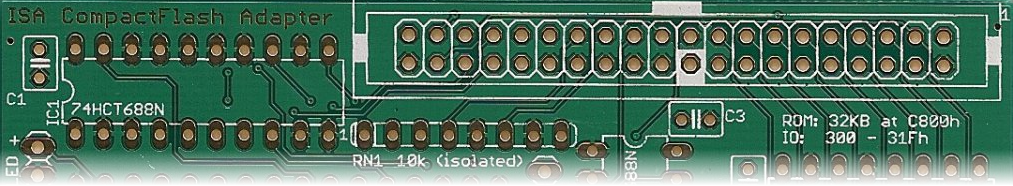
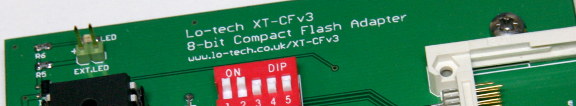
Now formally rev.3 and made in the UK, the PCB features a thicker, 2.5µm gold card-edge connector for long-term durability as well as ENIG finish for easy soldering and bevelled edge.
The design also includes ROM address selection, PC/XT slot-8 functionality with disable jumper, and more durable power supply for key-pin powered DoM and CompactFlash adapters with an optional 2.2uF tantalum capacitor at the header.
The SMT components on the back of the board remain optional, meaning this design is still the cheapest, easiest to assemble, fastest, and most compatible storage adapter for PC and PC/XT class hardware.
I was contacted recently by the owner of a Sinclair PC200 (an XT class machine in an Atari ST style case) about my XT-CF boards, wondering if a custom board could be built for the machine, with its physical 50mm height restriction on its two ISA slots. The quick answer to that is no, since the CompactFlash header is too big in either orientation, but I’d already been pondering on the idea of a super-simple PCB providing a 40-pin IDE header, based on the lo-tech 8-bit ROM board, so this seemed like a good opportunity to finish the design.
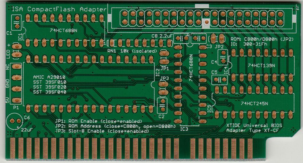
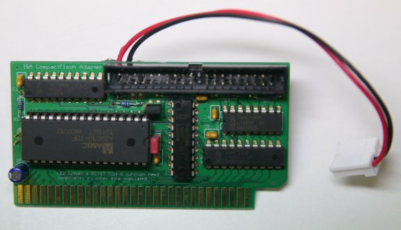
A through-hole, small form factor 8-bit ISA adapter providing a 40-pin IDE header suitable for connection to a separate IDE to CompactFlash adapter (available cheaply on eBay). By using a 40-pin header instead of a CompactFlash socket, home assembly of the device is made simple as all required components are 2.54mm pitch through-hole.
Other than the small form factor (and without any provision for a slot bracket), the PCB is a standard ISA card and can be used in any PC with an ISA slot.
New IDE Logic Implementation
Making an XT/IDE derivative in such a small PCB meant minimising the component count:
Whilst the XT-CF-lite was based closely on the original XT/IDE adapter, borrowing directly its OR and inverter gate design to provide IDE register access and IDE reset, with this new board this has been condensed into a single 74LS139.
Because of the 40-pin potentially cabled connection to the CompactFlash adapter, a buffer (74HCT245) is required, but with only 8-bit transfer mode supported (hence the CompactFlash designation), a 16-to-8-bit MUX isn’t required
Any CompactFlash or microdrive device should work with this adapter, and probably ATA-2 compliant hard drives (since 8-bit transfer mode is a requirement of ATA-2).
Extended Functionality
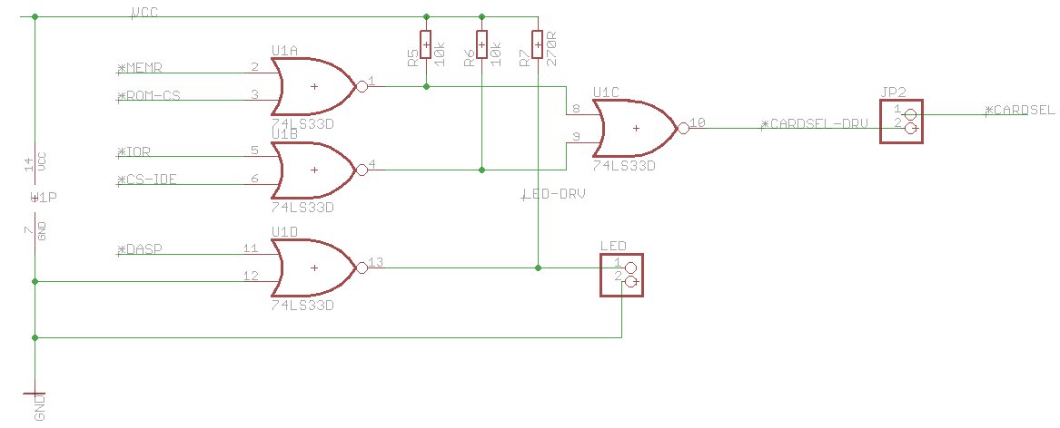
I wanted to include as much functionality as possible, so implementing the logic for IBM PC/XT Slot-8 compatibility (developed with the CPLD based XT-CF adapters) was a goal. Although out of space on the ISA component side, the layout could accommodate a few SMT components on the ISA solder side: these are entirely optional, but when populated provide LED drive and Slot-8 functions.
The logic required to provide slot-8 functionality is straight-forward – it’s just an echo of MEMR or IOR when either the ROM or IDE ports (respectively) are selected, with an open-collector drive since other logic on the system board can also drive this signal (as I’ve written about before). In this new board, this is implemented with a single 74LS33D quad NOR gate, the one spare gate being used to provide LED drive too:
LED drive requires the SMT 74LS33D populated since CompactFlash devices provide only minimal activity LED drive current, which is likely already absorbed by LEDs on the required CompactFlash to IDE adapter.
The boards are fully supported by the XTIDE Universal BIOS (from build R545), with standard 8-bit PIO transfer mode and the enhanced performance BIU Offload mode just as with the XT-CF-lite. The DMA transfer mode of the XT-CFv3 is not however supported.
Availability
ENIG (gold plated) rev.2 PCBs are available via the shop page.
Components will also be needed from your local electronics outlet such as Farnell, Mouser or Digikey – full Bill of Materials in the wiki.
The XT-CFv3 DMA transfer mode works in an unconventional way to deliver the highest possible throughput for the original IBM PC and PC/XT – here’s how.
The Intel 8237 DMA Controller
In the PC and PC/XT, the Intel 8237 DMA controller provides two functions – it keeps system memory alive by periodic refresh, and it enables transfers to and from IO devices with minimal CPU intervention (the floppy drive, many hard disk controllers, and SoundBlaster cards use DMA). To achieve this, the DMA controller has four sets of DMA Request (DRQ) and DMA Acknowledge (DACK) lines and broadly, the process is:
DRQ is asserted by the requesting IO device (e.g. the floppy drive controller)
The DMA controller raises the HOLD line (connected to the 8088 CPU)
The 8088 CPU completes the current bus cycle, then asserts HLDA (Hold Acknowledge) so passing control to the DMA controller. At this point, all output lines on the CPU are put in a high-Z state (effectively disconnected) and the CPU enters a waiting state
Now the DMA controller has control of the bus, it presents the memory address on the address bus and asserts AEN, which signals to IO devices not involved in the DMA transfer to disregard the bus cycle
The DMA controller next asserts DACK, preparing the IO device to present (or receive) data
Then the DMA controller asserts both IOR (IO read) and MEMW (memory write) concurrently, or IOW (IO write) and MEMR (memory read), so feeding data directly from the device to memory or vice-versa
The DMA controller transfer counter and memory address registers are then updated
What happens next depends on whether more data is available (so DRQ is still asserted), whether the transfer counter has reached zero, and finally the DMA controller operating mode. In single byte transfer mode, the DMA controller will return control to the CPU by releasing HOLD after each byte, whilst in demand mode the process will continue until the IO device releases DRQ (block mode generally isn’t used because it can disrupt RAM refresh, as described below).
DMA vs Port IO
In demand mode DMA runs much faster than 8088/V20 transfers since with DMA, each byte is delivered to memory in just one bus cycle. The 8088, on the other hand, has to read the byte from the IO device in one bus cycle then store it to memory in a second bus cycle, because both the IO device and memory use the same address bus. On the 8088, the code to fetch a block of port mapped data is less than ideal:
mov cx, 512
 .TransferLoop:
 in al, dx
 stosb
 loop .TransferLoop
The instruction fetch and jumps of course make this slow, although it can be improved by unrolling. In the XTIDE Universal BIOS, this is the basis of the 8-bit port-mapped IO operating mode for the XT-CF series, achieving about 170KB/s at 4.77MHz. The V20 though streamlines this by eliminating instruction fetch and jump overhead:
mov cx, 512
 rep insb
Freeing up the bus for just the data by the elimination of all the instructions pays significant dividends – this delivers about 390KB/s at 4.77MHz (and is available in the ‘XTplus’ XTIDE Universal BIOS build, for V20/286 powered XT class hardware).
Making DMA Scream
DMA on the PC and PC/XT brings with it some challenges:
Programming the DMA controller absorbs many cycles
Control must be returned to the CPU every 15 µs (72 cycles) for RAM refresh
To play sampled SoundBlaster audio at 22KHz, the DMA controller must be available to service the SoundBlaster DRQ once every 216 cycles
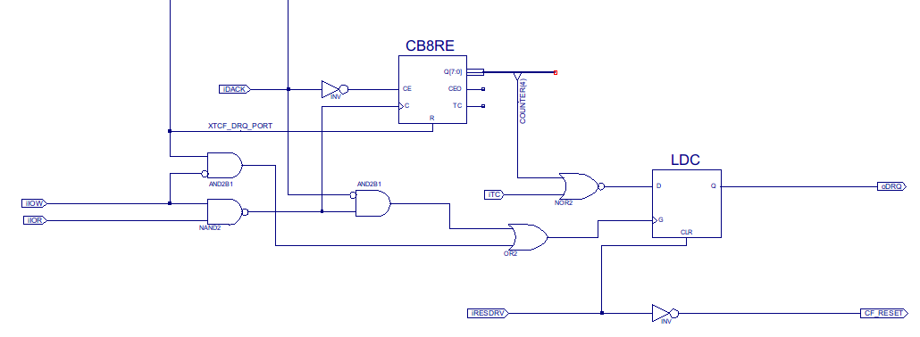
For my goal of ultimate throughput, packing bytes back-to-back on the data bus is the key – and with each byte taking 4 cycles, 18 bytes can be transferred before disrupting RAM refresh. For the XT-CFv3, this is achieved with some counter logic to release DRQ after 16 bytes (since that makes the maths easy and provides a margin of safety):
In the XT-CFv3, the oDRQ output in the schematic is delivered to the ISA bus via a 3-state output buffer, because the card must be able to co-exist with any original hard disk controller and DMA channels (DRQ/DACK pairs) can’t be shared as there are no pull-ups on the DRQ lines, so the card must drive the line continually when DMA function is in use.
Generating DRQ
Because DRQ is released by the counter, the DRQ lines on the IDE interface can’t be used – and in any case, DMA isn’t even supported by the majority of CompactFlash cards. The XT-CFv3 therefore provides another mechanism – to allow the software direct control over DRQ through an IO port write (the address decoding for which appears in the schematic above as ‘XTCF_DRQ_PORT’). This approach makes the transfer code itself elegant, once the DMA controller has been programmed:
mov cx, 32
 .TransferNextDmaBlock:
 out        dx, al                ; Raise XT-CFv3 DRQ & transfer 16 bytes
 loop    .TransferNextDmaBlock    ; loop also adds required wait-state
The results are heavily dependent on the media: the majority of CompactFlash cards support only single-sector transfers, and therefore the DMA controller must be programmed once for every 512 bytes transferred, which delivers about 420 KB/s – a vast improvement on 8-bit port IO. But for devices supporting multi-sector transfers, performance rises to 530KB/s with an 8088 and a 560KB/s with a V20 (both at 4.77MHz).
Since working on the Dangerous Prototypes version of the XT/IDE project, I’ve been increasingly interested in ‘the storage problem’ for early 1980’s PCs – it’s both difficult to transfer files between machines and increasingly problematic storing data on them too, with still surviving hard drives now well into borrowed time.
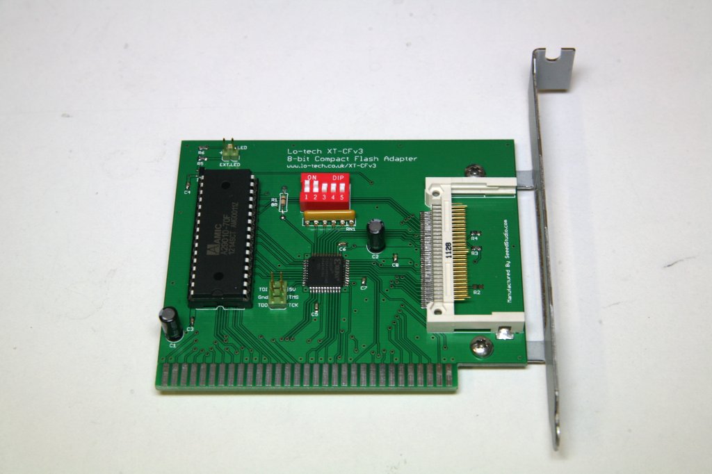
The goal was to make a board with the DMA function of the XT-CFv2, but as easy to make as the XT-CF-lite (only the CompactFlash header represents something of a soldering challenge). So the XT-CFv3 specs:
8-bit ISA card providing bootable fixed-disk storage for PC/XT and PC/AT class hardware
Up to 8GB usable by MS-DOS (DOS limit)
CompactFlash header positioned to allow CompactFlash media to be exchanged through a custom ISA card slot, without opening the PC
32KB in-system re-programmable flash ROM, providing storage for the XTIDE Universal BIOS boot ROM with 24KB free
Provides several transfer modes optimised for 8088, V20 and 286 machines
Up to 530KB/s in a stock PC/XT, and up to 1.1.MB/s in a 12MHz 286
Low-cost manufacturing requirements
Programmable Logic: the Xilinx XC9536
At the heart of the XT-CFv3 is the Xilinx XC9536 CPLD. To me, these are little pieces of silicon magic – simply hook up the components on the PCB to the nearest convenient CPLD pin, then define in software the circuit logic the CPLD should perform and upload it into the CPLD. This is great for home-brew projects like this, since once the basic PCB layout is done and the board electrically sound, the design can be revised over-and-over by just reprogramming the CPLD.
The XT-CFv3 logic is a greatly simplified version of that from the XT-CFv2, which aside from electrical reliability issues, was working well enough – so I was confident the logic would work. Even so, six revisions were needed to finally bring the thing to life. But it’s running now with three modes of operation – more on which will follow soon 🙂
DMA Transfers
DMA is the big XT-CFv3 feature: it offers performance way beyond what any disk controller ‘back in the day’ could do, achieving up to 530KB/s on a stock PC/XT. The CPLD implementation makes this possible since it can do the work of many discrete logic chips (and of course be reprogrammed in the development phase getting it running). More on this, and the other operating modes, to follow soon.
Availability
The XT-CFv3 is just entering field testing so is some way off still. The plan though is to offer bare PCBs and brackets for home assembly.
Beta testing of the XT-CFv2 has uncovered some compatibility and reliability issues that will take time to fix, so in the mean time – and conscious of the long development time already of these boards – I’ve turned my attention to making a simpler, more home-assembler friendly XT-CF derivative.
Surface-mount (SMT), especially the 0.5mm pitch components, seem to have put off home-assemblers, and then there’s the need to program the CPLD. Though SMT can’t be avoided because of the CompactFlash header, using SOIC chips but still in the same PCB footprint (and ISA slot bracket), things can be made a lot easier.
Just like the XT-CFv2, it’s a self-contained ISA disk device, functionally like a hard-card, providing solid-state, bootable storage to any PC with an ISA slot – right back to the original IBM PC 5150.
What Gives?
This board provides the same basic functionality of the XT-CFv2 – a 32K (accessible) flash-based ROM (with 24KB available for any user purposes), XTIDE Universal BIOS support and the port-based IO transfer mode used by the XT-CFv2 by default. But there are some limitations, because the CPLD on the XT-CFv2 provides a wealth of logic space not present here, so the lite version misses out on BIOS port auto-detection, memory-mapped IO, DMA, slot-8 compatibility, and reduced-wait-state operation for PC/AT and above.
No Buffer?
Usually a buffer chip like the 74LS245 would be used between the ISA bus and the media, but I took a chance that one isn’t needed, because the CF card is directly connected (i.e. not cabled) and has 8mA output drive strength. And luckily, it seems to work!
That’s SMT – wasn’t is supposed to be easier to make?
We can’t get away from SMT and still use CompactFlash – through-hole sockets do exist on datasheets, but are near impossible to find. Compared to the XT-CFv2:
0.5mm lead-pitch flash chip has been replaced with an easy through-hole DIP package, and the 100-pin CPLD has been eliminated altogether
1206 package resistor networks have been replaced with a through-hole network
And of course there’s no CPLD programming to do once it’s assembled. The activity LED and driver IC (IC6) can be left-off if need be. The tiny 0603 package capacitors and resistors remain but are also quite easy. The hardest part is the CF header, but locating points on the header hold it in position whilst it’s soldered, and the trick is to use plenty of flux and flow solder over the pins generously, then use solder wick and more flux to clean up the job.
How Fast?
With the official XTIDE Universal BIOS, it will do about 150-180KB/s on a PC/XT. It’s possible to increase this about 20% by switching the BIOS to 16-bit IO cycles, but at the expense of system compatibility. 16-bit port IO is faster because it reduces the instruction count and off-loads some work to the bus interface unit (BIU), but in development of the XT-CFv2 it was found that some clones have errors in BIU logic resulting in byte-swapped data delivery.
This website uses cookies to improve your experience. We'll assume you're ok with this, but you can opt-out if you wish.AcceptRead More
Privacy & Cookies Policy
Privacy Overview
This website uses cookies to improve your experience while you navigate through the website. Out of these, the cookies that are categorized as necessary are stored on your browser as they are essential for the working of basic functionalities of the website. We also use third-party cookies that help us analyze and understand how you use this website. These cookies will be stored in your browser only with your consent. You also have the option to opt-out of these cookies. But opting out of some of these cookies may affect your browsing experience.
Necessary cookies are absolutely essential for the website to function properly. This category only includes cookies that ensures basic functionalities and security features of the website. These cookies do not store any personal information.
Any cookies that may not be particularly necessary for the website to function and is used specifically to collect user personal data via analytics, ads, other embedded contents are termed as non-necessary cookies. It is mandatory to procure user consent prior to running these cookies on your website.
Lo-tech products are sold via TexElec. Please visit their web site texelec.com. Dismiss