Since working on the Dangerous Prototypes version of the XT/IDE project, I’ve been increasingly interested in ‘the storage problem’ for early 1980’s PCs – it’s both difficult to transfer files between machines and increasingly problematic storing data on them too, with still surviving hard drives now well into borrowed time.
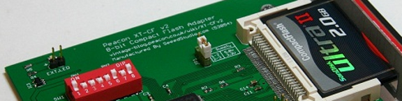
My first attempt (the XT-CF board) was too limited to justify the assembly effort, and my second attempt (the XT-CFv2 board) pushed the 3.3V CPLD too far so suffering reliability issues. Next I created the simpler XT-CF-lite, which Sergey has taken on and improved with his re-spin, using mostly through-hole components.
So the CPLD based project was apparently dead, until some 5V XC9536 CPLDs popped up again on Farnell (supply is sporadic but more are due): the XT-CFv3 board was born:
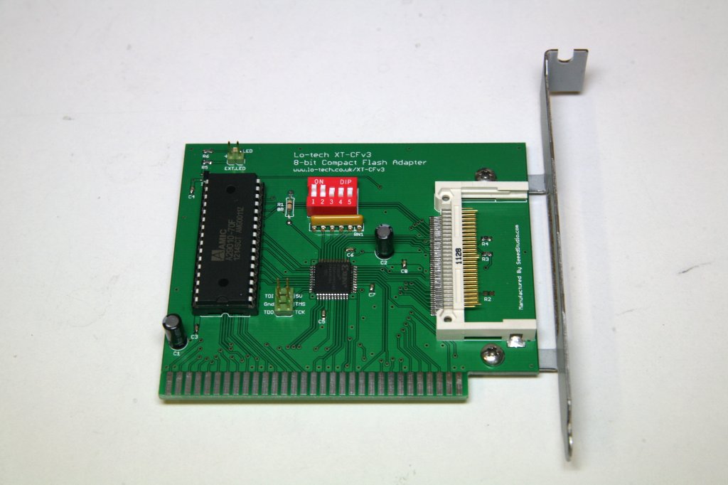
The goal was to make a board with the DMA function of the XT-CFv2, but as easy to make as the XT-CF-lite (only the CompactFlash header represents something of a soldering challenge). So the XT-CFv3 specs:
- 8-bit ISA card providing bootable fixed-disk storage for PC/XT and PC/AT class hardware
- Up to 8GB usable by MS-DOS (DOS limit)
- CompactFlash header positioned to allow CompactFlash media to be exchanged through a custom ISA card slot, without opening the PC
- 32KB in-system re-programmable flash ROM, providing storage for the XTIDE Universal BIOS boot ROM with 24KB free
- Provides several transfer modes optimised for 8088, V20 and 286 machines
- Up to 530KB/s in a stock PC/XT, and up to 1.1.MB/s in a 12MHz 286
- Low-cost manufacturing requirements
Programmable Logic: the Xilinx XC9536
At the heart of the XT-CFv3 is the Xilinx XC9536 CPLD. To me, these are little pieces of silicon magic – simply hook up the components on the PCB to the nearest convenient CPLD pin, then define in software the circuit logic the CPLD should perform and upload it into the CPLD. This is great for home-brew projects like this, since once the basic PCB layout is done and the board electrically sound, the design can be revised over-and-over by just reprogramming the CPLD.
The XT-CFv3 logic is a greatly simplified version of that from the XT-CFv2, which aside from electrical reliability issues, was working well enough – so I was confident the logic would work. Even so, six revisions were needed to finally bring the thing to life. But it’s running now with three modes of operation – more on which will follow soon 🙂
DMA Transfers
DMA is the big XT-CFv3 feature: it offers performance way beyond what any disk controller ‘back in the day’ could do, achieving up to 530KB/s on a stock PC/XT. The CPLD implementation makes this possible since it can do the work of many discrete logic chips (and of course be reprogrammed in the development phase getting it running). More on this, and the other operating modes, to follow soon.
Availability
The XT-CFv3 is just entering field testing so is some way off still. The plan though is to offer bare PCBs and brackets for home assembly.
In the mean time, Sergey has done a great job with his version of the XT-CF-lite, making it mostly through-hole so a little easier to make.


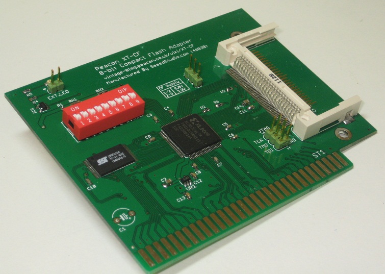

 So going completely against the survey, my card as it exists today has only a CF slot, mounted so the CF card is accessible through the expansion slot bracket (but not hot-pluggable). Originally based on the DPv2, there’s now little left in the design from it other than the CPLD choice (the Xilinx XC9572XL). By replacing the EEPROM with


")